우리는 반도체 산업에서 반도체 웨이퍼의 전문가, 우리는 기술 지원 및 코넬 대학, 스탠포드 Univeristy, 북경 대학, 산동 Univerity, 사우스 캐롤라이나의 대학, 캘리포니아 공과 대학을 포함하여 우리의 수십 년간의 경험에 의해 univerisities 수천 산업 고객을위한 판매 웨이퍼를 제공 Faraon 연구소 (USA)캘리포니아 어바인 (미국), 연구 및 기술 센터 싱가포르 MIT 연합 (SMART), 웨스트 버지니아 대학, 퍼듀 Univerity, 캘리포니아 대학, 로스 앤젤레스, 과학 기술의 압둘라 국왕 대학, 기술 대학의 매사 추세 츠 공과 대학 휴스턴, 위스콘신 대학, 중국 등의 과학 기술 대학
그리고 지금 우리는 우리의 웨이퍼이나 서비스를 구입 한 사람, 한 문서의 예로서 다음과 보여
기사 제목 :
나노 구조의 GaN에서의 Ag (0001): 형태학 진화는 박막의 솔리드 스테이트 탈 적심 및 해당 광학 속성에 의해 제어
에 의해 출판 됨:
다르 Kunwar1, 마오 Sui1, Quanzhen Zhang1, Puran Pandey1, 명나라 유 인 Li1 및 전자 정보의 지훈 Lee1,2 * 1College, 광운대 학교, 노원구 서울 01897, 나노 과학 및 공학, 아칸소 대학의 한국 2Institute, 페이 어트 빌 AR 72701, USA.
질화 갈륨 웨이퍼의 사진 :
추상
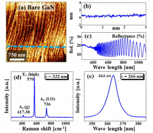
Silver (Ag) nanostructures have demonstrated the feasibility of being utilized in various optoelectronic, catalytic, biomedical, and sensor devices due to their excellent surface plasmon resonance characteristics. The geometrical structure, spacing, and spatial arrangement of nanostructures are crucial for controlling the properties and device performance. Herein, we demonstrate the fabrication of various configurations of self-assembled Ag nanostructures on GaN (0001) by the systematic control of deposition thickness and annealing duration. The surface morphology evolution is thoroughly investigated, and the corresponding influence on optical properties is probed. The evolution of Ag nanostructures in response to thermal annealing is described based on the dewetting of thin films, Volmer–Weber growth model, coalescence growth, and surface energy minimization mechanism. For the deposition amount variation between 1 and 100 nm, the Ag nanostructures show gradual morphological transitions such as small nanoparticles (NPs) to enlarged NPs between 1 and 7 nm, elongated nanostructures to cluster networks between 10 and 30 nm, and void evolution with layered nanostructures between 40 and 100 nm. In addition, the annealing duration effect has been studied between 0 and 3600 s, where the Ag nanostructures exhibit the evolution of network-like, elongated and isolated irregular shapes, ascribed to Ostwald’s ripening along with Ag sublimation. Furthermore, corresponding Raman, photoluminescence, and reflectance spectra reveal the morphology-dependent behaviors and are discussed based on the phonon, emission band, scattering, absorption, and surface plasmon effect.
하문 Powerway 고급 재료 유한 회사 (PAM-하문) 또는 Powerway 웨이퍼 유한 제한에서 웨이퍼를 사용하기위한 기술 추상적
"2.1의 GaN 기판의 제조. 우선, n 형 두께 5㎛의 GaN 에피 택셜 템플릿 "... 축외 ± 하문 Powerway 신소재 주식회사 (PAM-XIAMEN, 중국)를 0.1 °와 650 ㎛의 두께의 사파이어 상에 성장 된
출처 :
https://pubs.acs.org/doi/abs/10.1021/acs.cgd.6b01185
하문 Powerway 고급 재료 유한 공사 소개
1990 년에 발견 하문 Powerway 고급 재료 유한 공사 (PAM-하문)는 중국의 화합물 반도체 재료의 선도적 인 제조 업체입니다. PAM-XIAMEN 고급 크리스탈 성장 에피 택시 기술의 제조 공정 설계의 기판 및 반도체 장치를 개발하고있다. PAM-XIAMEN의 기술은 높은 성능 및 반도체 웨이퍼의 제조 비용 절감을 가능하게한다.
지금 GaN 기판, 증착 속도, 다양한 도핑 레벨, 넓은 조성 범위의 넓은 범위와 사파이어의 GaN, InGaN으로 여관, AlN의 에피 택셜 웨이퍼와 낮은 결함 밀도를 포함 PAM-XIAMEN 쿠폰의 GaN 재료. 뿐만 아니라, GaN 계 LED 웨이퍼 또는 AlGaN / GaN으로 HEMT 웨이퍼.
PAM-XIAMEN은 에피 택셜 성장을 웨이퍼 기판에서의 SiC와 갈륨 비소 / InP의 물질을 제공한다.
Powerway 웨이퍼 유한 제한 하문 Powerway 고급 재료 유한의 하위 회사, 회사는 해외 수주를 다루는 전문.
당신은 반도체 웨이퍼를 찾고 계십니까?
PAM-XIAMEN 아닙니다 반도체 웨이퍼를 자랑 inlcuidng의 SiC / GaN으로 / 갈륨 비소 / InP의 웨이퍼와 웨이퍼 또는 프로젝트의 모든 다른 종류의 에피 택셜 웨이퍼. 당신은 반도체 웨이퍼를 찾고 있다면, 우리는 당신이 당신의 다음 프로젝트에 필요한 기판 웨이퍼를 얻기 위해 당신과 함께 작업 할 수있는 방법에 대해 자세히 알아 오늘 저희에게 문의 보냅니다. 우리 그룹 팀은 당신을 위해 품질의 제품과 우수한 서비스를 모두 제공하기 위해 기대하고 있습니다! 자세한 내용은 저희 웹 사이트를 방문하십시오 :www.powerwaywafer.com에서 우리에게 이메일을 보내tech@powerwaywafer.com또는powerwaymaterial@gmail.com.