当社は、半導体業界における半導体ウエハの専門家であり、我々はコーネル大学、スタンフォードUniveristy、北京大学、山東Univerity、サウスカロライナ大学、カリフォルニア工科大学など、私たちの数十年の経験でuniverisitiesおよび産業分野のお客様の数千人のための販売、技術サポートおよびウェハを提供しますファラオンラボ(USA)カリフォルニア大学アーバイン校(USA)、研究技術センター(SMART)、ウェストバージニア大学、パデューUniverity、カリフォルニア大学ロサンゼルス校、科学技術、テクノロジー、大学のマサチューセッツ工科大学のアブドラ国王大学のためにシンガポールMITアライアンスヒューストン、ウィスコンシン大学、中国などの科学技術大学の
次のようにそして今、我々は我々のウエハーやサービスを買って誰が、1つの記事の例を示します。
記事タイトル:
GaN上のAgナノ構造(0001):薄膜のソリッドステートディウェッティングと対応する光学特性によって制御された形態の進化
発行:
サンダーKunwar1、真央SUI1、Quanzhen Zhang1、Puran Pandey1、明ゆうたLi1および電子情報のJihoon Lee1,2 * 1College、光云大学校、蘆原区ソウル01897、ナノスケール科学工学、アーカンソー大学の韓国2Institute、フェイエットビルAR 72701、USA。
窒化ガリウムウエハの写真:
抽象
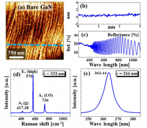
Silver (Ag) nanostructures have demonstrated the feasibility of being utilized in various optoelectronic, catalytic, biomedical, and sensor devices due to their excellent surface plasmon resonance characteristics. The geometrical structure, spacing, and spatial arrangement of nanostructures are crucial for controlling the properties and device performance. Herein, we demonstrate the fabrication of various configurations of self-assembled Ag nanostructures on GaN (0001) by the systematic control of deposition thickness and annealing duration. The surface morphology evolution is thoroughly investigated, and the corresponding influence on optical properties is probed. The evolution of Ag nanostructures in response to thermal annealing is described based on the dewetting of thin films, Volmer–Weber growth model, coalescence growth, and surface energy minimization mechanism. For the deposition amount variation between 1 and 100 nm, the Ag nanostructures show gradual morphological transitions such as small nanoparticles (NPs) to enlarged NPs between 1 and 7 nm, elongated nanostructures to cluster networks between 10 and 30 nm, and void evolution with layered nanostructures between 40 and 100 nm. In addition, the annealing duration effect has been studied between 0 and 3600 s, where the Ag nanostructures exhibit the evolution of network-like, elongated and isolated irregular shapes, ascribed to Ostwald’s ripening along with Ag sublimation. Furthermore, corresponding Raman, photoluminescence, and reflectance spectra reveal the morphology-dependent behaviors and are discussed based on the phonon, emission band, scattering, absorption, and surface plasmon effect.
アモイPowerwayアドバンストマテリアル株式会社(PAM-厦門)またはPowerwayウェーハ株式会社、株式会社からウエハを使用するための抽象条
「2.1のGaN基板の準備。 最初に、n型の厚さ5μmのGaNテンプレートをエピタキシャルオフアクシス±0.1と650ミクロンの厚さのサファイアの上に成長させた°アモイPowerwayアドバンストマテリアル株式会社(PAM-厦門、中国)...」で
出典:
https://pubs.acs.org/doi/abs/10.1021/acs.cgd.6b01185
アモイPowerwayアドバンストマテリアル株式会社について
1990年に発見、アモイPowerwayアドバンストマテリアル株式会社(PAM-厦門)は、中国における化合物半導体材料のリーディングカンパニーです。 PAM-厦門は、高度な結晶成長およびエピタキシー技術、製造工程、操作基板および半導体装置を開発します。 PAM-厦門の技術は、より高いパフォーマンスと半導体ウエハの低コストの製造を可能にします。
今GaN基板、堆積速度、様々なドーピングレベル、広い組成範囲の広い範囲でサファイア上のGaN、InGaN系、インとAlNエピタキシャルウエハ、及び低欠陥密度を含むPAM-厦門オファーGaN材料。 同様にGaN系LEDウェハとのAlGaN / GaN HEMTウェハ。
PAM-厦門も、エピタキシャル成長にウエハ基板からのSiC及びGaAs / InP系材料を提供します。
Powerwayウェーハ株式会社は、株式会社は、アモイPowerwayアドバンストマテリアル株式会社のサブ会社である、株式会社は、海外の受注を扱うに特化。
あなたは、半導体ウェハをお探しですか?
PAM-厦門は、プロジェクトのすべての異なる種類のウエハやエピタキシャルウェーハを提供する半導体ウェハinlcuidngのSiC / GaN系/ GaAs系/ InP基板に誇りに思っています。 あなたは、半導体ウェハを探しているなら、我々はあなたがあなたの次のプロジェクトのために必要な基板ウェーハを得るためにあなたと一緒に働くことができる方法についての詳細を学ぶために、今日私たちにお問い合わせを送信。 当社グループのチームがあなたのための高品質な製品と優れたサービスの両方を提供することを楽しみにしています! 詳細については、当社のウェブサイトをご覧ください。www.powerwaywafer.com、で私達に電子メールを送りますtech@powerwaywafer.com若しくはpowerwaymaterial@gmail.com.