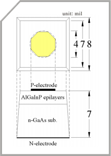
PAM-XIAMEN offers SiC-on-SiC epi wafer for pin-diodes (p-n junction SiC epi wafer) as follows:
SiC-On-SiC Epi Wafer For Pin-Diodes
1. Specifications of SiC Epitaxy on Silicon Carbide Substrate
pin-diodes structure 1: SiC-on-SiC epi-wafer PAM060320-SIC
p+[Al]: 5 µm, gradient doping, Na-Nd = 5*10^18 – 1*10^20 ± 50% cm-3
p[Al]: [...]
2020-08-04메타 작성자
PAM XIAMEN offers 2″ Prime Silicon Wafer Tnickness 675 +/- 20 microns.
2 inch in diameter wafers
Monocrystalline silicon with insulating oxide
Polishing: one-sided for microelectronics
Thickness: 675 +/- 20 microns
TTV <15 microns,
Warping <35 microns
For more information, please visit our website: [...]
2019-07-01메타 작성자
Rectifier is a controllable rectifier device based on controllable silicon (thyristor) and centered on intelligent digital control circuits, which converts AC to DC. It is abbreviated as silicon rectifier, also known as thyristor rectifier, thyristor rectifier, etc. Silicon rectifier advantages include high efficiency, no mechanical noise and wear, [...]
2023-10-10메타 작성자
PAM XIAMEN offers Si+SiO2+Pt Thin Film.
Si+SiO2+Pt Thin Film
SiO2+Pt thin film on Si (B-doped)substrate ,10x10x0.5mm,1sp (SiO2=500nm, Pt=60nm)
Silicon Wafer Specifications:
Conductive type: SiO2+Pt thin film on Si (B-doped, (100)Ori.) substrate ,10x10x0.5mm,1sp( SiO2=500nm,Pt=60nm)
Resistivity: [...]
2019-05-16메타 작성자
PAM XIAMEN offers high-quality Al2O3 (Sapphire).
Al2O3(10-14)
Al2O3- Sapphire Wafer, (10-14), 10x10x0.5mm, 1 SP
Fearures:
Sapphire substrate is the popular substrates for III-V nitrides, superconductor and magnetic epi film due to less mis-matched lattice and stable chemical and physical properties.
Wafer size: 10 [...]
2019-04-16메타 작성자
PAM-XIAMEN offers (20-21) Plane Si-GaN Freestanding GaN Substrate
Item
PAM-FS-GAN(20-21)-SI
Dimension
5 x 10 mm2 or 5 x 20 mm2
Thickness
380+/-50um
Orientation
(20-21)/(20-2-1) plane off angle toward A-axis 0 ±0.5°
(20-21)/(20-2-1) plane off angle toward C-axis -1 ±0.2°
Conduction Type
Semi-Insulating
Resistivity (300K)
> 106 Ω.cm
TTV
≤ 10 µm
BOW
BOW ≤ 10 µm
Surface Roughness:
Front side: Ra<0.2nm, epi-ready;
Back side: Fine Ground or polished.
Dislocation Density
≤5 x 106 cm-2
Macro Defect Density
0 cm-2
Useable Area
> 90% (edge exclusion)
Package
each in single wafer container, under nitrogen atmosphere, packed in class 100 clean room
For more information, please contact us email at victorchan@powerwaywafer.com and powerwaymaterial@gmail.com
2020-08-20메타 작성자