Ge (Gecmani) Crystal Độc thân và Quế
- Sự miêu tả
Mô Tả Sản Phẩm
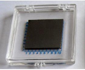
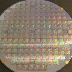
Wafer Germanium đơn tinh thể
PAM-XIAMEN cung cấp wafer germanium 2”, 3”, 4” và 6”, viết tắt của wafer Ge do VGF / LEC phát triển. Cũng có thể sử dụng wafer Germanium loại N và P pha tạp nhẹ cho thí nghiệm hiệu ứng Hall. Ở nhiệt độ phòng, gecmani kết tinh giòn và ít dẻo. Germanium có tính chất bán dẫn.Gecmani tinh khiết caođược pha tạp với các nguyên tố hóa trị ba (như indi, gali, bo) để thu được chất bán dẫn gecmani loại P; và các nguyên tố hóa trị năm (chẳng hạn như antimon, asen và phốt pho) được pha tạp để thu được chất bán dẫn germani loại N. Germanium có các đặc tính bán dẫn tốt, chẳng hạn như độ linh động của điện tử cao và độ linh động của lỗ trống cao.
1. Tính chất của bánh xốp Germanium
1.1 Tính chất chung của wafer Germanium
| Cấu trúc chung Thuộc tính | Khối, a = 5.6754 Å | ||
| Mật độ: 5,765 g / cm3 | |||
| Điểm nóng chảy: 937,4 oC | |||
| Dẫn nhiệt: 640 | |||
| Công nghệ tinh thể tăng trưởng | Czochralski | ||
| doping sẵn | / | Sb Doping | Doping nhập hoặc Ga |
| Loại dẫn | N | N | P |
| Điện trở suất, ohm.cm | >35 | <0,05 | 0,05-0,1 |
| EPD | <5 × 10³ / cm2 | <5 × 10³ / cm2 | <5 × 10³ / cm2 |
| <5 × 10² / cm2 | <5 × 10² / cm2 | <5 × 10² / cm2 | |
1.2 Các loại và Ứng dụng của wafer Germanium
| Lớp điện tử | Sử dụng cho các điốt và transistor, |
| Lớp hồng ngoại hoặc opitical | Sử dụng cho cửa sổ quang IR hoặc đĩa, linh kiện opitical |
| Lớp tế bào | Được sử dụng cho chất nền của pin mặt trời |
1.3 Thông số kỹ thuật tiêu chuẩn của Germanium Crystal và wafer
| Định hướng tinh | <111>,<100> và <110> ± 0,5o hoặc hướng tùy chỉnh | |||
| Tinh boule như đã trưởng thành | 1 "~ 6" đường kính x 200 mm Chiều dài | |||
| trống tiêu chuẩn như cắt | 1 "x 0.5mm | 2 "x0.6mm | 4 "x0.7mm | 5 "& 6" x0.8mm |
| Chuẩn wafer đánh bóng (Một / Hai bên đánh bóng) | 1 "x 0.30 mm | 2 "x0.5mm | 4 "x0.5mm | 5 "& 6" x0,6 mm |
- Kích thước và định hướng đặc biệt có sẵn theo yêu cầu
2. Thông số kỹ thuật của wafer Germanium
2.1 Thông số kỹ thuật của wafer Germanium có kích thước 2”,3”,4” và 6”
| Mục | Đặc tính kỹ thuật | Các chú thích |
| Phương pháp phát triển | VGF | — |
| Loại dẫn | loại n, loại p | |
| dopant | Gallium hoặc Antimon | — |
| wafer Diamter | 2, 3,4 & 6 | inch |
| Định hướng tinh | (100), (111), (110) | — |
| Độ dày | 200 ~ 550 | um |
| HÀNH | EJ hoặc Mỹ | — |
| Carrier Nồng độ | yêu cầu khi khách hàng | |
| Điện trở tại RT | (0,001 ~ 80) | Ohm.cm |
| Etch Pit Mật độ | <5000 | / cm2 |
| Laser Marking | theo yêu cầu | — |
| Kết thúc bề mặt | P / E hay P / P | — |
| Epi sẵn sàng | Vâng | — |
| gói | Độc wafer container hoặc băng cassette | — |
2.2 Tấm wafer germanium cho pin mặt trời
| 4 inch Ge wafer Thông số kỹ thuật | cho tế bào năng lượng mặt trời | - |
| doping | P | - |
| doping chất | Ge-Ga | - |
| Đường kính | 100 ± 0,25 mm | - |
| Sự định hướng | (100) 9 ° tắt hướng <111> +/- 0,5 | |
| góc nghiêng off-định hướng | N / A | - |
| Định hướng Flat chính | N / A | - |
| Tiểu Chiều dài phẳng | 32 ± 1 | mm |
| Định hướng Flat Secondary | N / A | - |
| Chiều dài phẳng THCS | N / A | mm |
| cc | (0,26-2,24) E18 | / cc |
| Điện trở | (0,74-2,81) E-2 | ohm.cm |
| electron Mobility | 382-865 | cm2 / vs |
| EPD | <300 | / cm2 |
| Laser Đánh dấu | N / A | - |
| Độ dày | 175 ± 10 | mm |
| TTV | <15 | mm |
| TIR | N / A | mm |
| CÂY CUNG | <10 | mm |
| Làm cong | <10 | mm |
| Đối mặt | đánh bóng | - |
| Mặt sau | Đất | - |
2.3 Ge wafer (làm chất nền bộ lọc quang học cho bộ lọc SWIR đường dài)
PAM180212-GE
| Mục | DSP Ge Wafer |
| Dia | 4" |
| Độ dày | 1,50mm +/- 0,10mm |
| Sự định hướng | N / A |
| Độ dẫn nhiệt | N / A |
| Điện trở | N / A |
| Quy trình bề mặt | Đánh bóng hai mặt; đường kính tối thiểu 90mm. khẩu độ trung tâm rõ ràng |
| Các thông số khác | 60-40 đầu đào hoặc tốt hơn |
| Ít hơn 2 phút cung song song | |
| Các bề mặt phẳng về mặt quang học trong phạm vi 1 rìa không đều trên bất kỳ đường kính 25mm nào. trong khẩu độ rõ ràng |
2.4 Gecmani được sử dụng làm cửa sổ FIR mỏng (PAM211121-GE)
Tấm wafer Germanium 4 inch với tần số plasma thấp, 175µm+/-25um. (100), đánh bóng một mặt.
3. Quy trình Wafer Germanium
Với sự tiến bộ của khoa học và công nghệ, kỹ thuật xử lý của các nhà sản xuất wafer germanium ngày càng hoàn thiện hơn. Trong quá trình sản xuất tấm mỏng germanium, germani dioxit từ quá trình xử lý cặn được tinh chế thêm trong các bước khử trùng bằng clo và thủy phân.
1) độ tinh khiết cao germanium thu được trong quá trình lọc dầu khu vực.
2) Một tinh thể germanium được sản xuất thông qua quá trình Czochralski.
3) Các wafer germanium được sản xuất thông qua một số cắt, mài, và các bước khắc.
4) Các tấm được làm sạch và kiểm tra. Trong quá trình này, các tấm là một mặt bên đánh bóng hoặc đánh bóng đôi theo yêu cầu tùy chỉnh, wafer epi-ready đến.
5) Các tấm mỏng germanium được đóng gói trong các thùng chứa tấm wafer duy nhất, trong môi trường khí nitơ.
4. Ứng dụng của Germanium:
Gecmani trống hoặc cửa sổ được sử dụng trong tầm nhìn ban đêm và các giải pháp hình ảnh nhiệt để cho an ninh thương mại, phòng chống cháy nổ và thiết bị giám sát công nghiệp. Ngoài ra, chúng được sử dụng như các bộ lọc cho các thiết bị phân tích và đo lường, cửa sổ để đo nhiệt độ từ xa, và gương cho laser.
Chất nền Germanium mỏng được sử dụng trong pin mặt trời ba lớp tiếp giáp III-V và cho các hệ thống năng lượng mặt trời tập trung (CPV) và làm chất nền bộ lọc quang học cho ứng dụng bộ lọc SWIR đường dài.
5. Kiểm tra Germanium Wafer:
Điện trở suất của wafer germanium tinh thể được đo bằng Máy kiểm tra điện trở bốn đầu dò và độ nhám bề mặt của germani được đo bằng máy đo cấu hình.
Nhận xét:
Chính phủ Trung Quốc đã công bố các giới hạn mới đối với việc xuất khẩu vật liệu Gallium (như GaAs, GaN, Ga2O3, GaP, InGaAs và GaSb) và vật liệu Germanium dùng để sản xuất chip bán dẫn vào ngày 3 tháng 7 năm 2023. Việc xuất khẩu những vật liệu này chỉ được phép nếu chúng tôi nhận được giấy phép từ Bộ Thương mại Trung Quốc. Rất mong sự thông cảm và hợp tác của bạn!

Để biết thêm thông tin, xin vui lòng liên hệ với chúng tôi email tạivictorchan@powerwaywafer.comvàpowerwaymaterial@gmail.com.
Bánh wafer Germanium mỏng loại P | Pin mặt trời
Chất nền Germanium cho quang học và tăng trưởng Epi
Cửa sổ Germanium (Ge) dạng cắt
Tinh thể Germanium (Ge) pha tạp hoặc không pha tạp | Tăng trưởng đơn tinh thể Ge
Bánh wafer Gecmani đơn tinh thể có hướng (110) về phía<111>
Phương pháp kiểm tra mật độ lệch vị trí của Germanium đơn tinh thể
Bạn cũng có thể thích…
-
GaN Templates
Mẫu Sản phẩm PAM-Hạ Môn của bao gồm lớp tinh thể (gallium nitride) GaN mẫu, (nhôm nitrua) mẫu AlN, (gallium nitride nhôm) mẫu AlGaN và (indium gallium nitride) mẫu InGaN, được lắng đọng trên sapphire -
CdZnTe (CZT) Wafer
Cadmium Kẽm Telluride (CdZnTe hoặc CZT) là một chất bán dẫn mới, cho phép chuyển đổi bức xạ để electron có hiệu quả, nó được sử dụng chủ yếu trong hồng ngoại màng mỏng epitaxy bề mặt, máy dò tia X và thiết bị dò tia gamma CdZnTe. -
InSb wafer
PAM-XIAMEN cung cấp wafer InSb bán dẫn hợp chất – wafer indium antimonide được phát triển bởi LEC (Liquid Encapsulated Czochralski) dưới dạng lớp sẵn sàng epi hoặc cơ học với loại n, loại p hoặc bán cách điện theo các hướng khác nhau(111) hoặc (100). Antimonua indi pha tạp với đẳng điện tử (như pha tạp N) có thể làm giảm mật độ khuyết tật trong quá trình sản xuất màng mỏng indi antimonua.
-
GaAs Epiwafer
PAM-XIAMEN đang sản xuất các loại vật liệu bán dẫn loại n pha tạp silicon epi III-V dựa trên Ga, Al, In, As và P do MBE hoặc MOCVD phát triển. Chúng tôi cung cấp các cấu trúc GaAs epiwafer tùy chỉnh để đáp ứng các thông số kỹ thuật của khách hàng, vui lòng liên hệ với chúng tôi để biết thêm thông tin.
-
Epitaxy Silicon wafer
Silicon Epitaxial Wafer (Epi Wafer) là một lớp silicon đơn tinh thể hình chóp được lắng đọng trên một wafer silicon đơn tinh thể (lưu ý: có thể phát triển một lớp silicon poly tinh thể lên trên một wafer silicon tinh thể Singly được pha tạp nhiều, nhưng nó cần lớp đệm (chẳng hạn như oxit hoặc poly-Si) ở giữa chất nền Si số lượng lớn và lớp silicon biểu mô trên cùng. Nó cũng có thể được sử dụng cho bóng bán dẫn màng mỏng.
-
GaN dựa LED epitaxy Wafer
GaN PAM-Hạ Môn của (gallium nitride) dựa trên LED wafer epitaxy là dành cho độ sáng cao điốt phát quang siêu màu xanh và màu xanh lá cây (LED) và điốt laser (LD) ứng dụng.
-
SiC wafer Substrate
Công ty có một dây chuyền sản xuất chất nền wafer SiC (silicon carbide) hoàn chỉnh tích hợp quá trình tăng trưởng tinh thể, xử lý tinh thể, xử lý wafer, đánh bóng, làm sạch và thử nghiệm. Ngày nay, chúng tôi cung cấp các tấm bán dẫn SiC 4H và 6H thương mại với tính năng bán cách điện và độ dẫn điện trên trục hoặc ngoài trục, kích thước có sẵn: 5x5mm2,10x10mm2, 2”,3”,4”, 6” và 8″, vượt qua các công nghệ chính như như loại bỏ khuyết tật, xử lý hạt tinh thể và tăng trưởng nhanh, thúc đẩy nghiên cứu và phát triển cơ bản liên quan đến epitaxy silic cacbua, thiết bị, v.v.
-
Thợ chụp ảnh chế tạo nano
PAM-Hạ Môn Cung cấp tấm cản quang với cản quang