Ge(Germanium) Single Crystals and Wafers
- Description
Product Description
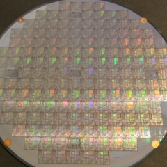
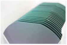
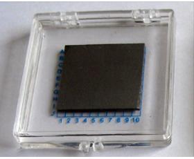
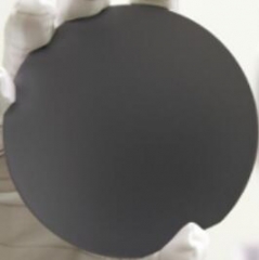
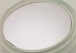
Single Crystal Germanium Wafer
PAM-XIAMEN offers 2”, 3”, 4” and 6” germanium wafer, which is short for Ge wafer grown by VGF / LEC. Lightly doped N and P type Germanium wafer can be also used for Hall effect experiment. At room temperature, crystalline germanium is brittle and has little plasticity. Germanium has semiconductor properties. High-purity germanium is doped with trivalent elements (such as indium, gallium, boron) to obtain P-type germanium semiconductors; and pentavalent elements (such as antimony, arsenic, and phosphorus) are doped to obtain N-type germanium semiconductors. Germanium has good semiconductor properties, such as high electron mobility and high hole mobility.
1. Properties of Germanium Wafer
1.1 General Properties of Germanium Wafer
| General Properties Structure | Cubic, a = 5.6754 Å | ||
| Density: 5.765 g/cm3 | |||
| Melting Point: 937.4 oC | |||
| Thermal Conductivity: 640 | |||
| Crystal Growth Technology | Czochralski | ||
| Doping available | / | Sb Doping | Doping In or Ga |
| Conductive Type | N | N | P |
| Resistivity, ohm.cm | >35 | < 0.05 | 0.05 – 0.1 |
| EPD | < 5×10³/cm2 | < 5×10³/cm2 | < 5×10³/cm2 |
| < 5×10²/cm2 | < 5×10²/cm2 | < 5×10²/cm2 | |
1.2 Grades and Application of Germanium wafer
| Electronic Grade | Used for diodes and transistors, |
| Infrared or opitical Grade | Used for IR optical window or disks,opitical components |
| Cell Grade | Used for substrates of solar cell |
1.3 Standard Specs of Germanium Crystal and wafer
| Crystal Orientation | <111>,<100> and <110> ± 0.5o or custom orientation | |||
| Crystal boule as grown | 1″ ~ 6″ diameter x 200 mm Length | |||
| Standard blank as cut | 1″x 0.5mm | 2″x0.6mm | 4″x0.7mm | 5″&6″x0.8mm |
| Standard Polished wafer(One/two sides polished) | 1″x 0.30 mm | 2″x0.5mm | 4″x0.5mm | 5″&6″x0.6mm |
- Special size and orientation are available upon requested Wafers
2. Specification of Germanium Wafer
2.1 Specification of Germanium Wafer of 2”,3”,4”and 6”size
| Item | Specifications | Remarks |
| Growth Method | VGF | — |
| Conduction Type | n-type, p type | |
| Dopant | Gallium or Antimony | — |
| Wafer Diamter | 2, 3,4 & 6 | inch |
| Crystal Orientation | (100),(111),(110) | — |
| Thickness | 200~550 | um |
| OF | EJ or US | — |
| Carrier Concentration | request upon customers | |
| Resistivity at RT | (0.001~80) | Ohm.cm |
| Etch Pit Density | <5000 | /cm2 |
| Laser Marking | upon request | — |
| Surface Finish | P/E or P/P | — |
| Epi ready | Yes | — |
| Package | Single wafer container or cassette | — |
2.2 Germanium Wafer for Solar Cell
| 4 inch Ge wafer Specification | for Solar Cells | — |
| Doping | P | — |
| Doping substances | Ge-Ga | — |
| Diameter | 100±0.25 mm | — |
| Orientation | (100) 9° off toward <111>+/-0.5 | |
| Off-orientation tilt angle | N/A | — |
| Primary Flat Orientation | N/A | — |
| Primary Flat Length | 32±1 | mm |
| Secondary Flat Orientation | N/A | — |
| Secondary Flat Length | N/A | mm |
| cc | (0.26-2.24)E18 | /c.c |
| Resistivity | (0.74-2.81)E-2 | ohm.cm |
| Electron Mobility | 382-865 | cm2/v.s. |
| EPD | <300 | /cm2 |
| Laser Mark | N/A | — |
| Thickness | 175±10 | μm |
| TTV | <15 | μm |
| TIR | N/A | μm |
| BOW | <10 | μm |
| Warp | <10 | μm |
| Front face | Polished | — |
| Back face | Ground | — |
2.3 Ge Wafer (as an optical filter substrate for a longpass SWIR filter)
PAM180212-GE
| Item | DSP Ge Wafer |
| Dia | 4” |
| Thickness | 1.50mm +/- 0.10mm |
| Orientation | N/A |
| Conductivity | N/A |
| Resistivity | N/A |
| Surface Process | Double-side polished; minimum 90mm dia. central clear aperture |
| Other Parameters | 60-40 scratch-dig or better |
| Less than 2 arc minutes parallelism | |
| Surfaces optically flat to within 1 fringe irregular per any 25mm dia. in the clear aperture |
2.4 Germanium Used as Thin FIR Window (PAM211121-GE)
4″ Germanium wafer with low plasma frequency, 175µm+/-25um. (100), single side polished.
3. Germanium Wafer Process
With the advancement of science and technology, the processing technique of germanium wafer manufacturers is more and more mature. In the production of germanium wafers, germanium dioxide from the residue processing is further purified in chlorination and hydrolysis steps.
1)High purity germanium is obtained during zone refining.
2)A germanium crystal is produced via the Czochralski process.
3)The germanium wafer is manufactured via several cutting, grinding, and etching steps.
4)The wafers are cleaned and inspection. During this process, the wafers are single side polished or double side polished according to custom requirement, epi-ready wafer comes.
5)The thin germanium wafers are packed in single wafer containers, under a nitrogen atmosphere.
4. Application of Germanium:
Germanium blank or window are used in night vision and thermographic imaging solutions for commercial security, fire fighting and industrial monitoring equipment. Also, they are used as filters for analytical and measuring equipment, windows for remote temperature measurement, and mirrors for lasers.
Thin Germanium substrates are used in III-V triple-junction solar cells and for power Concentrated PV (CPV) systems and as an optical filter substrate for a longpass SWIR filter application.
5. Test of Germanium Wafer:
The resistivity of the crystal germanium wafer was measured by Four Probe Resistance Tester, and the surface roughness of Germanium was measured by profilometer.
Remark:
The Chinese government has announced new limits on the exportation of Gallium materials (such as GaAs, GaN, Ga2O3, GaP, InGaAs, and GaSb) and Germanium materials used to make semiconductor chips on July 3, 2023. Exporting these materials is only allowed if we obtains a license from the Chinese Ministry of Commerce. Hope for your understanding and cooperation!

For more information, please contact us email at victorchan@powerwaywafer.com and powerwaymaterial@gmail.com.
P Type Thin Germanium Wafer | Solar Cell
Germanium Substrate for Optics and Epi-growth
Doped or Undoped Germanium (Ge) Crystal | Ge Single Crystal Growth
Single Crystal Germanium Wafer with Orientation (110) toward<111>
Test Method for Dislocation Density of Monocrystal Germanium
You may also like…
-
GaN based LED Epitaxial Wafer
PAM-XIAMEN’s GaN(gallium nitride)-based LED epitaxial wafer is for ultra high brightness blue and green light emitting diodes (LED) and laser diodes (LD) application.
-
SiC Wafer Substrate
The company has a complete SiC(silicon carbide) wafer substrate production line integrating crystal growth, crystal processing, wafer processing, polishing, cleaning and testing. Nowadays we supply commercial 4H and 6H SiC wafers with semi insulation and conductivity in on-axis or off-axis, available size:5x5mm2,10x10mm2, 2”,3”,4”, 6” and 8″, breaking through key technologies such as defect suppression, seed crystal processing and rapid growth, promoting basic research and development related to silicon carbide epitaxy, devices, etc.
-
GaN Templates
PAM-XIAMEN’s Template Products consist of crystalline layers of (gallium nitride)GaN templates, (aluminum nitride)AlN template,(aluminum gallium nitride) AlGaN templates and (indium gallium nitride) InGaN templates, which are deposited on sapphire -
Nanofabrication Photoresist
PAM-XIAMEN Offers photoresist plate with photoresist
-
Epitaxial Silicon Wafer
Silicon Epitaxial Wafer(Epi Wafer) is a layer of epitaxial silicon single crystal deposited onto a single crystal silicon wafer(note: it is available to grow a layer of poly crystalline Silicon layer on top of a highly doped Singly crystalline silicon wafer, but it needs buffer layer (such as oxide or poly-Si) in between the bulk Si substrate and the top epitaxial silicon layer. It also can be used for thin film transistor.
-
GaAs Epiwafer
PAM-XIAMEN is manufacturing various types of epi wafer III-V silicon doped n-type semiconductor materials based on Ga, Al, In, As and P grown by MBE or MOCVD. We supply custom GaAs epiwafer structures to meet customer specifications, please contact us for more information.
-
CdZnTe (CZT) Wafer
Cadmium Zinc Telluride (CdZnTe or CZT) is a new semiconductor, which enables to convert radiation to electron effectively, it is mainly used in infrared thin-film epitaxy substrate, X-ray detectors and Gamma-ray CdZnTe detectors. -
InSb wafer
PAM-XIAMEN offers Compound Semiconductor InSb wafer – Indium antimonide wafer which is grown by LEC(Liquid Encapsulated Czochralski) as epi-ready or mechanical grade with n type, p type or semi-insulating in different orientation(111) or (100). Indium antimonide doped with isoelectronic(such as N doping) can reduce the defect density during the indium antimonide thin films manufacturing process.