から販売されている単結晶ダイヤモンド PAM-厦門は、高温で水素と炭化水素ガスを炭化水素活性基に分解し、特定の条件下で基板材料上にダイヤモンドを堆積する方法である化学気相成長法 (CVD) によって成長します。 理論的には、このメソッドのサイズには制限がありません。 また、作製された電子レベル単結晶ダイヤモンドは、完全に無色透明で不純物がほとんど含まれない高品質なものとなる。 同時に、CVD単結晶ダイヤモンド成長プロセス中にドーピングガスを選択的に導入すると、多様な色のダイヤモンドを製造することができる。 CVDダイヤモンドには多くの利点があるため、ダイヤモンドウェーハは高出力エレクトロニクスや、通信、エネルギー、半導体、航空宇宙などの最先端分野の主要材料となっています。
ダイヤモンド基板の成長プロセスの詳細については、ビデオをご覧ください。 https://youtu.be/XQEFCeY06Do.
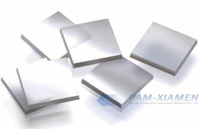
1.単結晶ダイヤモンドウェーハの仕様
PAM-210819-ダイヤモンド
| アイテム | 単結晶CVDダイヤモンドウェーハ |
| サイズ | 3x3mm2、7x7mm2 |
| 方向付け | (100)+/- 2度 |
| 厚さ | 200um +/- 25um |
| ロッキングカーブのピーク幅の半分 | <= 55arcsec |
| UV-Visスペクトルの270nmでの透過率 | > 50% |
| ラマンハーフピーク幅 | <= 2.8cm |
| 平面の並列処理 | <20um |
| 表面粗さ | <2nm |
| 表面処理 | 両面研磨 |
2.ダイヤモンドの材質特性
ダイヤモンドは、バンドギャップが5.5 eVの超ワイドバンドギャップ半導体材料であり、GaNやSiCなどのワイドバンドギャップ半導体材料よりも大きくなっています。 下の表に示すように、ダイヤモンドのバンドギャップはSiの5倍です。 キャリア移動度もSi材料の3倍です。 理論的には、ダイヤモンドのキャリア移動度は既存のキャリア移動度よりも高くなります ワイドバンドギャップ半導体材料 (GaN、SiC)。 また、2倍以上高くなっています。 一方、ダイヤモンドは室温での固有キャリア濃度が非常に低くなっています。 また、単結晶ダイヤモンドの熱伝導率は、硬度が最も高いことに加えて、半導体材料の中で最も高く、AlNの7.5倍です。 これらの優れた性能パラメータに基づいて、ダイヤモンドの単結晶は、次世代の高出力、高周波、高温、および低電力損失の電子デバイスの製造に最も有望な材料であると考えられています。
| 材料 | バンドギャップ幅eV | 固有のキャリア濃度cm-3 | 電子移動度cm2/ Vs | 電子飽和速度107cm / s | Breakdown Field Strength MV/cm | Thermal Conductivity W/cmK |
| Diamond | 5.47 | ~10-27 | 4500 | 1.5 | >20 | 22 |
| AlNの | 6.2 | ~10-31 | 1100 | 2.2 | 12 | 2.9 |
| Gallium Oxide | 4.8-5.0 | ~10-22 | 300 | – | 8 | 0.11/0.27 |
| GaN系 | 3.4 | ~10-10 | 2000 | 2.5 | 3.2 | 1.3 |
| SiC | 3.3 | ~10-9 | 950 | 2.0 | 3.0 | 4.9 |
| GaAs | 1.4 | 106 | 8500 | 2.0 | 0.4 | 0.43 |
| シ | 1.1 | 1010 | 1500 | 1.0 | 0.3 | 1.5 |
3. CVD Single Crystal Diamond Substrate Application in Semiconductor
The remarkable progress of single crystal diamond growth by chemical vapor deposition makes it possible to prepare diamond suitable for radiation detection on a conventional basis. With the continuous improvement of CVD method, it is possible to grow a large-area homoepitaxial single crystal CVD diamond plate / film. Single crystal diamond CVD wafer has broad application prospects, such as radio frequency diodes, bipolar junction transistors, field effect transistors, micro-electromechanical systems (MEMS) and electronics industry.
Due to the high atomic density of diamond, it is difficult to dope and conduct electricity, so the field effect transistor is mainly produced by hydrogen terminal surface conductance. However, the characteristics of diamond are very good. MoO3 is introduced, which is a transfer doping medium, under the gate of the hydrogen-terminated diamond field effect transistor. The forward conduction resistance is reduced to 1/3 of that of the MOSFET based on EL SC diamond wafer with the same gate length, and the transconductance is increased by approximately 3 times.
Single -crystal diamond wafers have made great progress in the power electronics in electrical vehicles and RF power technology for satellites and 5G communications.
特に、5G通信の時代は急速かつ包括的になり、半導体や高周波パワーデバイスへの単結晶バルクダイヤモンドの応用がますます顕著になっています。 大型用の単結晶ダイヤモンドは、超精密加工やスマートグリッドなどの主要な国家戦略の実施、およびスマート製造や5G通信などの産業クラスターのアップグレードのための重要な材料基盤です。 このため、ダイヤモンド材料の研究は、サイズが大きく、欠陥が少なく、抵抗率が低く、熱伝導率が高い方向に発展する必要があります。

詳細については、メールでお問い合わせください。 victorchan@powerwaywafer.com と powerwaymaterial@gmail.com.