Due to the high growth pressure and relatively low temperature, Al is not easily evaporated and lost in the liquid-phase method. Adding Al to the flux used in the liquid-phase method can easily obtain P-type silicon carbide (SiC) crystals with high carrier concentration, solving the problem of missing P-type silicon carbide substrate in the SiC industry. PAM-XIAMEN is able to supply liquid-phase grown p-type silicon carbide substrates, with properties such as low resistance, high doping concentration, and high quality. The p-type substrates can meet the preparation requirements of bipolar devices such as n-channel IGBT and GTO. Please refer to the following tables for specific specifications:
1. P-Type Silicon Carbide Substrate Specifications
1.1 50.8mm P-Type 4H/6H SiC Wafer
| Item | 2 inch P-Type SiC Substrate | |||
| Grade | Ultra Prime Grade | Industrial Grade | Test Grade | |
| 直径 | 50.8±0.38mm | |||
| 厚さ | 350±25um | |||
| Polytype | 4H or 6H | |||
| Orientation | off axis 2~4° toward [11-20]±0.5° | |||
| Primary Flat Orientation | {10–10}±5.0° | |||
| Primary Flat Length | 15.9±1.7mm | |||
| Secondary Flat Orientation | Si face up: 90° CW.from prime flat ±5.0° | |||
| Secondary Flat Length | 8.0±1.7mm | |||
| MPD* | <0.1cm-2 | |||
| Resistivity * | ≤0.1Ω·cm | ≤0.3Ω·cm | ||
| LTV | ≤2.5μm | |||
| TTV | ≤5μm | |||
| 弓 | ≤15μm | |||
| Warp | ≤25μm | ≤30μm | ||
| Roughness* | Polishing | Ra≤1nm | ||
| CMP | Ra≤0.2nm | Ra≤0.5nm | ||
| Edge Cracks by High Intensity Light | None | 1 allowed, ≤1mm | ||
| Hex Plates by High Intensity Light* | Cumulative area≤0.05% | Cumulative area≤3% | ||
| Polytype Areas by High Intensity Light* | None | Cumulative area≤5% | ||
| Visual Carbon Inclusions | Cumulative area≤0.05% | Cumulative area≤3% | ||
| Scratches on Si Face by High Intensity Light | None | 8 scratches to 1×wafer diameter cumulative length | ||
| Edge Chips by High Intensity Light | None permitted≥0.2mm width and depth | 5 allowed, ≤1mm each | ||
| Si-Face Contamination by High Intensity Light | None | |||
| Edge Exclusion | 1mm | 5mm | ||
| Package | Single Wafer Box or Multi Wafer Box | |||
“*” value is applicable to the entire wafer surface except for edge exclusion areas
1.2 100mm P-Type 4H-SiC Wafer
| Item | 4 inch P-Type 4H-SiC Substrate | |||
| Grade | Ultra Prime Grade | Industrial Grade | Test Grade | |
| 直径 | 99.5~100mm | |||
| 厚さ | 350±25um | |||
| Polytype | 4H | |||
| Orientation | off axis 2~4° toward [11–20]±0.5° | |||
| Primary Flat Orientation | {10–10}±5.0° | |||
| Primary Flat Length | 32.5±2.0mm | |||
| Secondary Flat Orientation | Si face up: 90° CW.from prime flat ±5.0° | |||
| Secondary Flat Length | 18.0±2.0mm | |||
| MPD* | <0.1cm-2 | |||
| Resistivity * | ≤0.1Ω·cm | ≤0.3Ω·cm | ||
| LTV | ≤2.5μm | ≤10μm | ||
| TTV | ≤5μm | ≤15μm | ||
| 弓 | ≤15μm | ≤25μm | ||
| Warp | ≤30μm | ≤40μm | ||
| Roughness* | Polishing | Ra≤1nm | ||
| CMP | Ra≤0.2nm | Ra≤0.5nm | ||
| Edge Cracks by High Intensity Light | None | Cumulative length≤10mm,single length≤2mm | ||
| Hex Plates by High Intensity Light* | Cumulative area≤0.05% | Cumulative area≤0.1% | ||
| Polytype Areas by High Intensity Light* | None | Cumulative area≤3% | ||
| Visual Carbon Inclusions | Cumulative area≤0.05% | Cumulative area≤3% | ||
| Scratches on Si Face by High Intensity Light | None | Cumulative≤1×wafer diameter | ||
| Edge Chips by High Intensity Light | None permitted≥0.2mm width and depth | 5 allowed, ≤1mm each | ||
| Si-Face Contamination by High Intensity Light | None | |||
| Edge Exclusion | 3mm | 6mm | ||
| Package | Single Wafer Box or Multi Wafer Box | |||
“*” value is applicable to the entire wafer surface except for edge exclusion areas
We just simplified introduce P-type silicon carbide substrate applications in IGBT ( Insulate-Gate Bipolar Transistor).
2. IGBT on P-Type SiC Substrate
IGBT = MOSFET + BJT、これは非オンまたはオフのスイッチです。 MOSFET = IGFET(金属酸化物半導体電界効果トランジスタ、または絶縁ゲート電界効果トランジスタ)。 BJT(バイポーラ接合トランジスタ、バイポーラ接合トランジスタ、三極真空管とも呼ばれます)、バイポーラは、動作中に伝導プロセスに関与する電子と正孔の両方が存在することを意味します。 一般に、伝導に関与するPN接合があります。
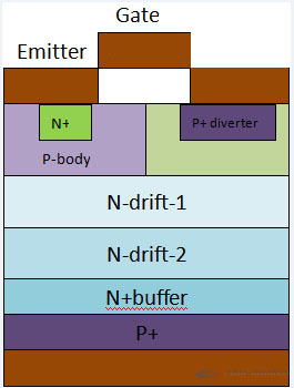
簡単な例を示します。上部を見ると、ゲート+エミッタ+ Nは完全に垂直MOSFET構造ですが、下部にP型半導体を追加してPNP型BJTを形成しています。
通電の原理は2つの部分に分かれています。
1)Voltage is applied to the gate, and the upper part is turned on, then the entire device is transformed into an NP structure from the top to the bottom.
2)Voltage is applied to the collector, so the lower half is turned on, and the PN junction is turned on normally.
最後に、電流はコレクターからエミッターに流れます。 PN接合が存在するため、電気を通す電子と正孔があります。
いくつか例を挙げてください。
上記の構造にワイヤを接続することで、IGBTシングルチューブとして使用できます。 外観はMSOFETに似ています。 結局のところ、それはスイッチとしても使用されます。
複数のIGBTを組み合わせたり、他のデバイスと組み合わせたりすると、IGBTモジュールとして使用できます。
IGBTは、低駆動電力や飽和電圧の低減など、BJTとMOSFETの利点を統合しています。
3. Development of SiC IGBT
炭化ケイ素IGBTの開発を以下に示します。
1996:最初の6H-SiCトレンチゲートIGBT
1999:最初の4H-SiCトレンチゲートpIGBT
2005年:最初の4H-SiCプレーナゲートnIGBT
2007:電荷蓄積層がJFET領域に導入されました
2010年:自立型技術の提案
2012:最初の12kV / 10A SiCIGBTモジュール
2015:* 15kV / 40AIGBTモジュール
*最初の7kV / 8kW SST
*最初の32kVマルクスジェネレータ
* 27kV SiC nIGBT
構造的に、IGBTには主に3つの開発方向があります。
1)縦方向構造:不透明コレクターエリアNPTタイプ、バッファー層PTタイプ、透明コレクターエリアNPTタイプ、FS電界カットオフタイプ。
2)ゲート構造:平面ゲート構造、トレンチ-トレンチ構造;
3)基板:エピタキシャル成長技術とタイプ。
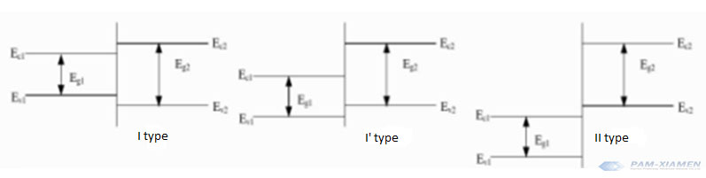
N型基板を用いたMOSFETの構造を継承するためには、P型炭化ケイ素基板上にIGBTを成長させる必要があります。 P型炭化ケイ素基板は、一般に、Alドープ炭化ケイ素基板を指す。 Alは+3価であり、SiCの+4価Siの一部を置き換え、Alと+1価の穴を形成します。 正孔はP型半導体です。 Alに加えて、B、Ga、Inなどの他の3価元素もP型ドーパントとして使用されます。 炭化ケイ素に窒素とリンをドープするとn型半導体が形成され、アルミニウム、ホウ素、ガリウム、ベリリウムをドープするとp型半導体が形成されます。 アルミニウムをドープした炭化ケイ素はタイプIIの半導体ですが、ホウ素をドープした炭化ケイ素はタイプIの半導体です。 ヘテロ接合のタイプは次のとおりです。タイプIヘテロ接合:小さな禁止バンドが大きな禁止バンドに囲まれています。 タイプⅠ 'ヘテロ接合:2つの禁止されたバンドが交差します。 タイプⅡヘテロ接合:2つの禁止されたバンドがずらされています。

詳細については、メールでお問い合わせください。victorchan@powerwaywafer.comそしてpowerwaymaterial@gmail.com.