
원자층 증착(ALD)에 대해 알아야 할 사항
원자층 에피택시(ALE)라고도 알려진 원자층 증착(ALD)은 원자 규모의 박막 준비 기술입니다. 균일한 두께, 조절 가능한 두께, 조절 가능한 구성으로 초박막 필름을 증착할 수 있습니다. 나노기술과 반도체 마이크로일렉트로닉스의 발달로 소자와 재료의 크기 요건은 지속적으로 감소하고, 소자 구조의 종횡비는 지속적으로 증가하여 사용되는 재료의 두께를 10나노미터에서 수 나노미터 정도로 줄여야 합니다. 나노미터. 원자층 증착 기술은 점차 관련 제조 분야에서 대체 불가능한 기술이 되었습니다. 그 장점은 개발 잠재력이 크고 응용 분야가 더 넓다는 점입니다. 금속 실리콘 웨이퍼ALD는 PAM-XIAMEN에서 제공할 수 있습니다.
1. 원자층 증착 기술의 작동 원리
원자층 증착 기술은 기상 전구체의 반응 챔버 내부로의 펄스와 증착 기판 표면의 기상-고상 화학 흡착 반응을 교대로 펄스화하여 박막을 형성하는 방법을 의미합니다. 그림 1에 표시된 것처럼 원자층 증착 공정은 4가지 기본 단계의 두 반쪽 반응 A와 B로 구성됩니다.
1) 전구체 A 펄스 흡착 반응;
2) 불활성 가스로 과잉 반응물 및 부산물을 퍼지하는 단계;
3) 전구체 B 펄스 흡착 반응;
4) The excess reactants and by-products are purged by the inert gas, and then circulated in sequence to realize the layer-by-layer growth of the thin film on the surface of the substrate.
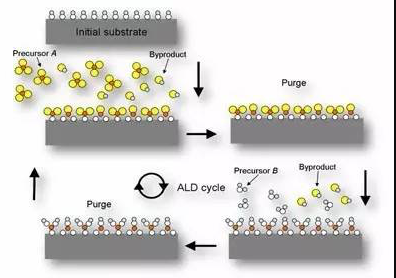
Figure 1. Working Principle of ALD
A wide variety of materials can be deposited by atomic layer deposition, such as:
Oxides: including HfO2, HfSiO, Al2O3, Ta2O5, TiO2, La2O3, SiO2, ZnO
Nitride, including TiN, TaN, AlN, SiNx, HfN
Metals, including Ru, Cu, W, Mo
2. Comparison of ALD, PVD and CVD
Compared with traditional thin film preparation technology, atomic layer deposition technology has obvious advantages. Traditional solution chemical methods and physical methods such as sputtering or evaporation (PVD) are not suitable for deposition and film formation on the surface of three-dimensional complex substrates due to lack of surface control or the existence of sputtered shadow areas. The chemical vapor deposition (CVD) method requires strict control of the precursor diffusion and the temperature uniformity of the reaction chamber, and it is difficult to meet the requirements of thin film uniformity and precise control of thickness. In contrast, ALD technology is based on surface self-limiting and self-saturating adsorption reactions, and has surface control. The bottom surface is deposited to form films, while still ensuring precise sub-monolayer film thickness control. Therefore, ALD technology is widely used in microelectronics, energy, information and other fields.
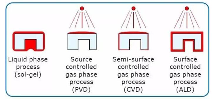
Figure 2. Comparison of ALD, PVD, CVD and so on
3. Basic Applications of Atomic Layer Deposition Technology
The development of atomic layer deposition technology is inseparable from the rise of the semiconductor industry. With the continuous improvement of chip integration, the size of various components continues to shrink, and the technology node of the semiconductor industry has entered the nano era. People also put forward higher and higher requirements for nano-scale thin film preparation technology compatible with semiconductor technology. The main applications of ALD technology include:
1) Transistor gate dielectric (high-k) and metalgate electrode;
2) Micro-electromechanical systems (MEMS);
3) Optoelectronic materials and devices;
4) Integrated circuit interconnect diffusion barrier;
5) Flat panel display (e.g. Organic light emitting diode material, OLED);
6) Interconnect barrier layer;
7) Interconnect copper electroplating deposition seed layer;
8) DRAM, MRAM dielectric layer;
9) Embedded capacitor;
10) Electromagnetic recording head;
11) Various types of thin films (<100nm).
자세한 내용은 이메일로 문의해 주세요.[email protected] 과 [email protected].