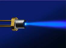
PAM-XIAMEN can offer 2” InGaN/GaN quantum well blue laser diode wafer on sapphire or silicon substrate as follows. The blue GaN LD wafer for commercial applications illustrates the great potential of III-V epitaxial wafers.
1. Specification of 440-460nm Blue GaN LD wafer
PAM190909-GAN-LD
| アイテム | 説明 | マテリアル | 基板 |
| 青色レーザー | 440-460nm | InGaN系 | 2 inch Sapphire substrate*** |
| GaN系青色LD EPIウェーハ仕様 | |||
| Spec | |||
| LD Epitaxial Wafer Size | |||
| 成長 | MOCVD | ||
| 直径 | 50.8±0.2ミリメートル | ||
| 厚さ | 430±30μmの | ||
| EPI厚さ | ええと | ||
| EPIウエハ構造 | |||
| コンタクト層 | p型GaN系 | ||
| 超格子クラッド層 | p型GaN系 | ||
| 電子ブロック層 | p型AlGaNから | ||
| 導波路層 | アンドープInGaN | ||
| QWとQB層 | InGaNとGaN | ||
| 導波路層 | n個のInGaNを入力 | ||
| クラッド層 | n個のAlGaNを入力 | ||
| 基板 | シリコン | ||
2. Structure of Blue Laser Diode Epitaxial Wafer
PAM-190130-LD
| substrates | t (nm) | 構成 | Doping | |||
| Al% | ln% | [Si] | [Mg] | |||
| uGaN | 2000-3000 | – | – | – | ||
| nGaN | – | – | – | – | – | |
| AlGaN | – | 6-10 | – | – | – | |
| lnGaN | – | – | – | – | – | |
| MQW (2pairs) |
lnGaN-QW | ~2.5 | – | – | – | – |
| GaN-QB | – | – | – | – | – | |
| lnGaN | – | – | 1-2 | – | – | |
| AlGaN | – | – | 1.OE+19 | |||
| pGaN | – | – | – | – | – | |
| コンタクト層 | 5 | – | – | – | – | |
3. GaN based Laser Diode Epitaxial Wafer, Blue Emission
PAM-191206–LD
|
Epitaxial Blue LD Structure with Emission Wavelength of 440~460nm |
||
| Layer Name | 材料 | 厚さ |
| Contact Layer | p-type GaN | 30nm |
| Superlattice Cladding Layer (80~150 pairs) | p-type GaN | – |
| p-type AlxxGaxxN | – | |
| Electron Blocking Layer (EBL) | p-type Al0.2Ga0.8N | – |
| 導波路層 | undoped In0.035Ga0.965N | – |
| MQW (xx pairs) | undoped GaN QB | – |
| InxxGaxxN QW | – | |
| 導波路層 | n-type InxxGaxxN | – |
| クラッド層 | n-type Al0.6Ga0.94N | 1.4um |
| 基板 | シリコン | |
4. Other Parameters
nternal Loss:Unknown
IQE: Unknow
Lifetime:xx seconds@CW, >10 hours@pulse mode
Peak Optical Power:xx mW@pulse mode.
The laser diode wafer process on silicon substrate is mainly by MOCVD method.
Please contact our technology dept to discuss blue GaN LD wafer specifications,including other wavelength, dimension, layer thickness and epitaxial design.

For more information, please contact us email at victorchan@powerwaywafer.com and powerwaymaterial@gmail.com.