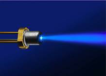
PAM-XIAMEN can offer 2” InGaN/GaN quantum well blue laser diode wafer on sapphire or silicon substrate as follows. The blue GaN LD wafer for commercial applications illustrates the great potential of III-V epitaxial wafers.
1. Specification of 440-460nm Blue GaN LD wafer
PAM190909-GAN-LD
| Item | Descriptions | Materials | Substrate |
| blue laser | 440-460nm | InGaN | 2 inch Sapphire substrate*** |
| GaN Blue LD EPI Wafer Spec | |||
| Spec | |||
| LD Epitaxial Wafer Size | |||
| Growth | MOCVD | ||
| Diameter | 50.8 ± 0.2 mm | ||
| Thickness | 430 ± 30 um | ||
| EPI thickness | um | ||
| EPI Wafer Structure | |||
| Contact layer | p type GaN | ||
| Superlattice Cladding Layer | p type GaN | ||
| Electron Blocking Layer | p type AlGaN | ||
| Waveguide Layer | undoped InGaN | ||
| QW and QB layer | InGaN and GaN | ||
| Waveguide Layer | n type InGaN | ||
| Cladding Layer | n type AlGaN | ||
| Substrate | Silicon | ||
2. Structure of Blue Laser Diode Epitaxial Wafer
PAM-190130-LD
| substrates | t (nm) | Composition | Doping | |||
| Al% | ln% | [Si] | [Mg] | |||
| uGaN | 2000-3000 | – | – | – | ||
| nGaN | – | – | – | – | – | |
| AlGaN | – | 6-10 | – | – | – | |
| lnGaN | – | – | – | – | – | |
| MQW (2pairs) |
lnGaN-QW | ~2.5 | – | – | – | – |
| GaN-QB | – | – | – | – | – | |
| lnGaN | – | – | 1-2 | – | – | |
| AlGaN | – | – | 1.OE+19 | |||
| pGaN | – | – | – | – | – | |
| Contact layer | 5 | – | – | – | – | |
3. GaN based Laser Diode Epitaxial Wafer, Blue Emission
PAM-191206–LD
|
Epitaxial Blue LD Structure with Emission Wavelength of 440~460nm |
||
| Layer Name | Material | Thickness |
| Contact Layer | p-type GaN | 30nm |
| Superlattice Cladding Layer (80~150 pairs) | p-type GaN | – |
| p-type AlxxGaxxN | – | |
| Electron Blocking Layer (EBL) | p-type Al0.2Ga0.8N | – |
| Waveguide Layer | undoped In0.035Ga0.965N | – |
| MQW (xx pairs) | undoped GaN QB | – |
| InxxGaxxN QW | – | |
| Waveguide Layer | n-type InxxGaxxN | – |
| Cladding Layer | n-type Al0.6Ga0.94N | 1.4um |
| Substrate | Silicon | |
4. Other Parameters
nternal Loss:Unknown
IQE: Unknow
Lifetime:xx seconds@CW, >10 hours@pulse mode
Peak Optical Power:xx mW@pulse mode.
The laser diode wafer process on silicon substrate is mainly by MOCVD method.
Please contact our technology dept to discuss blue GaN LD wafer specifications,including other wavelength, dimension, layer thickness and epitaxial design.

For more information, please contact us email at victorchan@powerwaywafer.com and powerwaymaterial@gmail.com.