自動車および産業エレクトロニクスの原動力により、炭化ケイ素 (SiC) パワー半導体市場は力強い成長を遂げ、今後数年間で 100 億ドルに近づくと予想されています。 同時に、多くの業界関係者が、市場シェアを迅速に獲得するために、対応する拡大計画を発表しました。 業界の主要参加者間の協力と統合により、炭化ケイ素のサプライチェーンが再構築されています。
業界参加者の一員として、PAM-XIAMEN は常に高性能パワー SiC ウェーハを供給することを目指しています。ウェーハ仕様の詳細については、以下をご覧ください。https://www.powerwaywafer.com/sic-wafer
1. 2022~2028 SiCウェーハ市場G列R食べました
Yole の Power SiC 2023 レポートによると、SiC パワー半導体市場は 2021 年の 11 億ドルから 2022 年には 18 億ドルに成長し、年間成長率は 62% です。 炭化珪素ウェーハ(6インチ相当)の出荷量は36万枚から57万枚に増加。
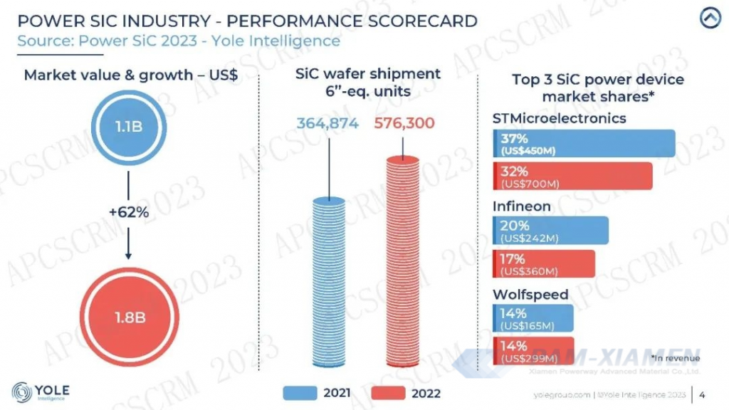
図 1 パワー SiC 業界 – パフォーマンス スコアカード
Yole は、SiC パワー半導体市場は 2022 年の 179 億ドルから 2028 年には 890 億ドルに成長し、年間平均成長率 (CAGR) は 31% になると予測しています。 そのうち、自動車エレクトロニクスと産業用エレクトロニクスが 85% 以上に貢献しています。
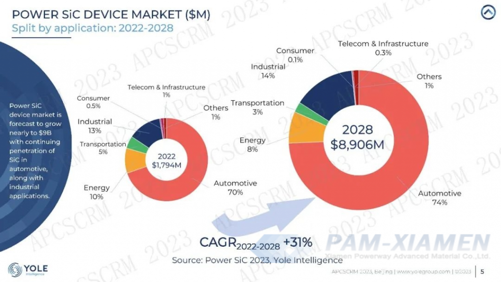
図2 パワーSiCデバイス市場
2. 2022年から2028年までのパワーSiCウェーハのコスト
SiC ウェーハの生産能力が継続的に増加するにつれて、デバイスの総コストに占めるウェーハコストの割合は減少し続けるでしょう。 Yoleは、SiCウェーハの生産歩留まりの向上と、より平面的な設計からトレンチ設計への移行などMOSFETデバイスの体積の減少により、SiCウェーハのコスト比率が2022年の30%から2028年には24%に減少すると予測しています。
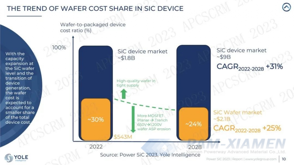
図3 SiCデバイスにおけるウェーハコストシェアの推移
The Bullwhip effect refers to the amplification phenomenon that occurs when the demand information of downstream enterprises in the industrial chain is transmitted to upstream enterprises. From the perspective of SiC wafer production capacity layout, there may be overcapacity in the future, and changes in downstream consumer market demand are likely to lead to significant fluctuations in SiC wafer inventory.
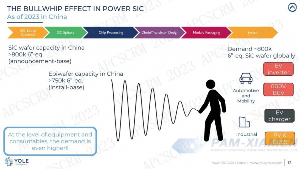
Fig. 4 The Bullwhip effect in power SiC
3. Market Analysis of 8inch SiC Wafers
The proportion of 8-inch SiC wafers is currently not high, which is closely related to the low yield and high cost of their production process. The expansion of production capacity for 6-inch silicon carbide wafers will bring economies of scale dividends, potentially lowering their costs to $700 per wafer.
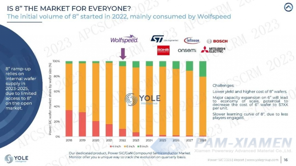
Fig. 5 Power SiC wafer market share by wafer size
The conversion of SiC wafers from 6 inches to 8 inches may seem to significantly reduce costs and bring rapid benefits, but in reality, there are still many hidden challenges. For example, increasing the thickness of an 8-inch wafer will reduce the utilization rate of the ingot; The low yield and high defect density of 8-inch SiC wafers pose obstacles to their large-scale application.
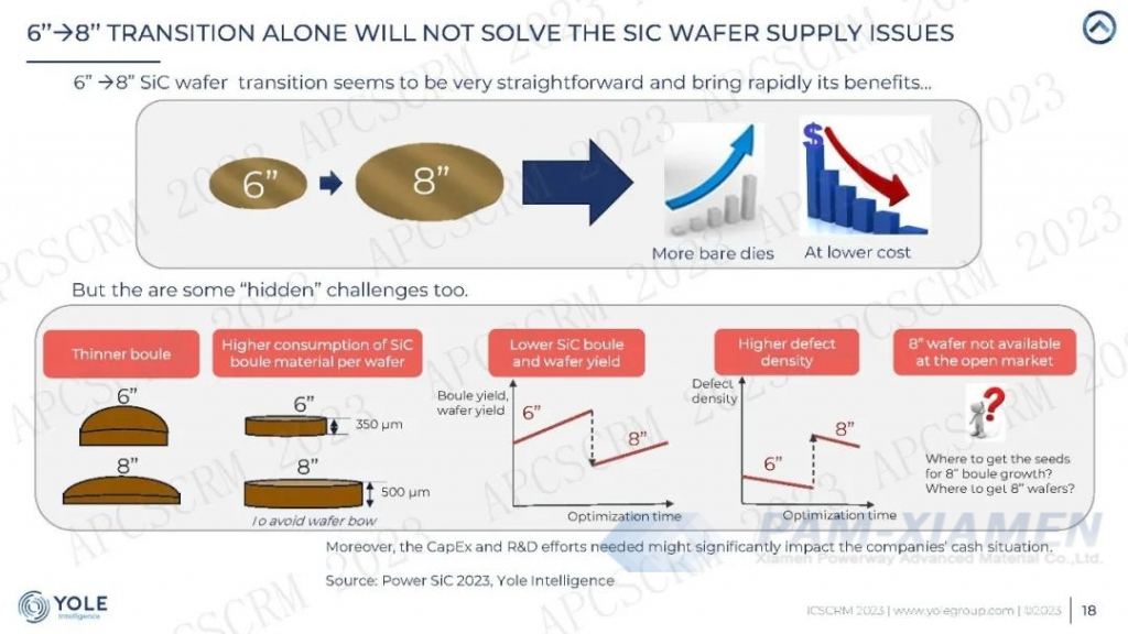
Fig. 6 Issues for transition of SiC wafer from 6 inches to 8 inches
6 インチ SiC ウェーハと比較すると、8 インチ SiC ウェーハには短期的な価格上の利点はありません。これは、コスト管理 (より高価)、技術の成熟度 (歩留まりの低下)、および市場の開放性 (より閉鎖的) と密接に関係しています。
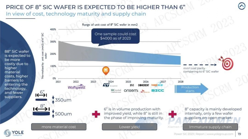
図7 8インチSiCウェハの価格

詳細については、メールでお問い合わせください。victorchan@powerwaywafer.com と powerwaymaterial@gmail.com.