
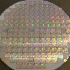
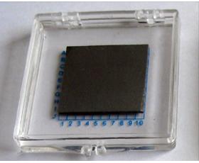
GaAs Epiwafer
PAM-XIAMEN is manufacturing various types of epi wafer III-V silicon doped n-type semiconductor materials based on Ga, Al, In, As and P grown by MBE or MOCVD. We supply custom GaAs epiwafer structures to meet customer specifications, please contact us for more information.
- Описание
Описание продукта
GaAs Epi wafer
As a leading GaAs epi wafer foundry, PAM-XIAMEN are manufacturing various types of epiwafer III-V silicon doped n-type semiconductor materials based on Ga, Al, In, As and P grown by MBE or MOCVD, which make a low gallium arsenide epi wafer defect. We supply custom GaAs epiwafer structures to meet customer specifications, please contact us for more information.
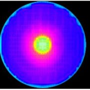
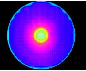
We have numbers of the United States Veeco’s GEN2000, GEN200 large-scale production of epitaxial equipment production line, full set of XRD; PL-Mapping; Surfacescan, and other world-class analysis and testing equipment. The company has more than 12,000 square meters of supporting plant, including world class super-clean semiconductor and a related research and development of the younger generation of clean laboratory facilities.
Specification for all new and featured products of MBE III-V compound semiconductor epitaxial wafer:
| Материал подложки | Материал Capability | Применение |
| GaAs | низкая температура GaAs | ТГц |
| GaAs | GaAs / GaAlAs / GaAs / GaAs | Диод Шоттки |
| InP | InGaAs | детектор PIN |
| InP | InP / InP / InGaAsP / InP / InGaAs | лазер |
| GaAs | GaAs / AlAs / GaAs | |
| InP | InP / InAsP / InGaAs / InAsP | |
| GaAs | GaAs / InGaAsN / AlGaAs | |
| / GaAs / AlGaAs | ||
| InP | InP / InGaAs / InP | фотоприемники |
| InP | InP / InGaAs / InP | |
| InP | InP / InGaAs | |
| GaAs | GaAs / InGaP / GaAs / AlInP | Солнечная батарея |
| / InGaP / AlInP / InGaP / AlInP | ||
| GaAs | GaAs / GaInP / GaInAs / GaAs / AlGaAs / GalnP / GalnAs | Солнечная батарея |
| / GalnP / GaAs / AlGaAs / AllnP / GalnP / AllnP / GalnAs | ||
| InP | InP / GaInP | |
| GaAs | GaAs / AlInP | |
| GaAs | GaAs / AlGaAs / GalnP / AlGaAs / GaAs | 703nm лазерный |
| GaAs | GaAs / AlGaAs / GaAs | |
| GaAs | GaAs / AlGaAs / GaAs / AlGaAs / GaAs | НЕМТ |
| GaAs | GaAs / AlAs / GaAs / AlAs / GaAs | mHEMT |
| GaAs | GaAs / DBR / AlGaInP / MQW / AlGaInP / GaP | Светодиодные пластины, твердотельное освещение |
| GaAs | GaAs / GalnP / AlGaInP / GaInP | 635nm, 660nm, 808nm, 780 нм, 785nm, |
| / GaAsP / GaAs / GaAs подложки | 950nm, 1300nm, 1550nm лазера | |
| GaSb | AlSb / GaInSb / InAs | ИК-детектор, PIN-код, зондирование, ИК cemera |
| кремний | InP или GaAs на кремнии | Высокая скорость IC / микропроцессоры |
| InSb | Бериллий легированного InSb | |
| / Нелегированный InSb / Te легированного InSb / |
Gallium arsenide is currently one of the most important compound semiconductor materials with the highest mature epi wafer technology. GaAs material has the characteristics of large forbidden band width, high electron mobility, direct band gap, high luminous efficiency. Due to all all these epi wafer advantages, GaAs epitaxy is currently the most important material used in the field of optoelectronics. Meanwhile, it is also an important microelectronic material. According to the difference in electrical conductivity, GaAs epi wafer materials can be divided into semi-insulating (SI) GaAs and semiconductor (SC) GaAs.
In the field of epitaxial wafers, the epi wafer market share of RF and laser applications is very large.
Для получения более подробной информации, пожалуйста, просмотрите следующее:
LT-GaAs EPI слой на подложке GaAs
LT GaAs Thin Film for Photodetectors and Photomixers
GaAs Шоттки диод эпитаксиальные Вафли
InGaAs / InP эпи вафельные для PIN
InGaAsP / InGaAs на InP подложках
InGaAs APD Wafers with High Performance
InGaAsN эпитаксиально на GaAs или InP вафель
Структура для InGaAs фотоприемников
InP / InGaAs / InP эпи вафельные
AlGaP / GaAs Epi вафельные для солнечных батарей
Triple-ответвительные солнечные батареи
Solar Cell Structure Epitaxially Grown on InP Wafer
Growth of GaAsSb / InGaAs Type-II Superlattice
AlGaAs / GaAs PIN Epitaxial Wafer
1550nm GaInAsP / InP PIN Photodiode Structure
GaAs / AlGaAs / GaAs EPI вафельные
Сейчас мы перечислим некоторые спецификации:
| GaAs HEMT epiwafer, size:2~6inch | ||
| Пункт | Характеристики | замечание |
| параметр | Аль Композиция / В составе сопротивление / Лист | Пожалуйста, свяжитесь с нашим отделом технологий |
| Подвижность зал / 2DEG Концентрация | ||
| Измерение технологий | Рентгеноструктурный / вихревой ток | Пожалуйста, свяжитесь с нашим отделом технологий |
| Un-контактный зал | ||
| Типичный клапан | Struture зависит | Пожалуйста, свяжитесь с нашим отделом технологий |
| 5000 ~ 6500cm2 / В · S / 0.5 ~ 1.0x 1012cm-2 | ||
| Стандартный допуск | не ± 0,01 / ± 3% / нет | Пожалуйста, свяжитесь с нашим отделом технологий |
| GaAs (арсенид галлия) pHEMT epiwafer, size:2~6inch | ||
| Пункт | Характеристики | замечание |
| параметр | Аль Композиция / В составе сопротивление / Лист | Пожалуйста, свяжитесь с нашим отделом технологий |
| Подвижность зал / 2DEG Концентрация | ||
| Измерение технологий | Рентгеноструктурный / вихревой ток | Пожалуйста, свяжитесь с нашим отделом технологий |
| Un-контактный зал | ||
| Типичный клапан | Struture зависит | Пожалуйста, свяжитесь с нашим отделом технологий |
| 5000 ~ 6800cm2 / В · S / 2.0 ~ 3.4x 1012cm-2 | ||
| Стандартный допуск | не ± 0,01 / ± 3% / нет | Пожалуйста, свяжитесь с нашим отделом технологий |
| Remark:GaAs pHEMT: Compared with GaAs HEMT, GaAs PHEMT also incorporates InxGa1-xAs,where InxAs is constrained to x < 0.3 for GaAs-based devices. Structures grown with the same lattice constant as HEMT, but different band gaps are simply referred to as lattice-matched HEMTs. | ||
| GaAs mHEMT epiwafer, size:2~6inch | ||
| Пункт | Характеристики | замечание |
| параметр | В композиции сопротивления / Sheet | Пожалуйста, свяжитесь с нашим отделом технологий |
| Подвижность зал / 2DEG Концентрация | ||
| Измерение технологий | Рентгеноструктурный / вихревой ток | Пожалуйста, свяжитесь с нашим отделом технологий |
| Un-контактный зал | ||
| Типичный клапан | Struture зависит | Пожалуйста, свяжитесь с нашим отделом технологий |
| 8000~10000cm2/V ·S/2.0~3.6x 1012cm-2 | ||
| Стандартный допуск | ± 3% / нет | Пожалуйста, свяжитесь с нашим отделом технологий |
| InP HEMT epiwafer, size:2~4inch | ||
| Пункт | Характеристики | замечание |
| параметр | В композиции / сопротивление листа / мобильность Холла | Пожалуйста, свяжитесь с нашим отделом технологий |
Remark: GaAs(Gallium arsenide) is a compound semiconductor material,a mixture of two elements, gallium (Ga) and arsenic (As). The uses of Gallium arsenide are varied and include being used in LED/LD, field-effect transistors (FETs), and integrated circuits (ICs)
приложения устройств
RF Switch, Power and low-noise amplifiers, Hall sensor, Оптический модулятор
Беспроводной: мобильный телефон или базовые станции
Automotive radar, MMIC, RFIC, Оптические волоконные коммуникации
GaAs Epi вафельные для LED / IR серии:
1.Общие Описание:
1.1 Метод роста: MOCVD
1.2 GaAs epi wafer for Wireless Networking
1,3GaAs EPI вафельные для LED/ ИК и LD / PD
2.Epi вафельные спецификации:
2.1 Вафли размер: 2” диаметр
2.2 GaAs Epi Wafer Structure(from top to bottom):
P + GaAs
п-GaP
п-AlGaInP
MQW-AlGaInP
н-AlGaInP
DBR n-ALGaAs / AlAs
Буфер
подложка GaAs,
3.Chip Sepcification (Base на 9mil * 9mil чипы)
3,1 Параметр
Chip Размер 9mil * 9mil
Толщина 190 ± 10um
Диаметр электрода 90um ± 5um
3.2 Оптико-Elctric символов (Ir = 20 мА, 22 ℃)
Длина волны 620 ~ 625nm
Прямое напряжение 1,9 ~ 2.2V
Обратный ≥10v напряжение
Обратный ток 0-1uA
3.3 символов интенсивности света (Ir = 20 мА, 22 ℃)
IV (MCD) 80-140
3.4 Epiwafer avelength
|
Пункт |
Ед. изм |
Красный |
Желтый |
Желто-зеленый |
Описание |
|
Длина волны (λD) |
нм |
585615620 ~ 630 |
587 ~ 592 |
568 ~ 573 |
IF = 20 мА |
Методы роста: MOCVD, MBE
эпитаксия = рост пленки с кристаллографической связью между пленкой и подложкой гомоэпитаксии (автоэпитаксии, isoepitaxy) = пленки и подложки являются такой же материал гетероэпитаксия = пленки и подложки различные материалы. Длябольше информации о методах роста, пожалуйста, нажмите на следующие:https://www.powerwaywafer.com/technology.html
Remark:
The Chinese government has announced new limits on the exportation of Gallium materials (such as GaAs, GaN, Ga2O3, GaP, InGaAs, and GaSb) and Germanium materials used to make semiconductor chips. Starting from August 1, 2023, exporting these materials is only allowed if we obtains a license from the Chinese Ministry of Commerce. Hope for your understanding and cooperation!
InGaAs Epitaxy Sensor / Detector:
Shortwave Infrared InGaAs Sensor
InGaAs/InAlAs Epistucture for Single Photon Detector
Epiwafer for Photonic Integrated Chip:
Эпитаксия тонкой пленки AlGaAs для фотонных интегральных чипов
Вам также может понравиться ...
-
Float-Zone монокристаллического кремния
PAM-XIAMEN может предложить кремниевую пластину с зоной плавания, полученную методом зоны плавания. Монокристаллические кремниевые стержни получают путем выращивания в зоне плавания, а затем перерабатывают монокристаллические кремниевые стержни в кремниевые пластины, называемые кремниевыми пластинами с плавающей зоной. Поскольку кремниевая пластина зонной плавки не контактирует с кварцевым тиглем во время процесса плавления кремния, кремниевый материал находится во взвешенном состоянии. Тем самым он меньше загрязняется в процессе зонной плавки кремния. Содержание углерода и кислорода ниже, примесей меньше, удельное сопротивление выше. Он подходит для производства силовых устройств и некоторых высоковольтных электронных устройств.
-
GaAs (арсенид галли) Вафли
As a leading GaAs substrate supplier, PAM-XIAMEN manufactures Epi-ready GaAs(Gallium Arsenide) Wafer Substrate including semi-conducting n type, semi-conductor C doped and p type with prime grade and dummy grade. The GaAs substrate resistivity depends on dopants, Si doped or Zn doped is (0.001~0.009) ohm.cm, C doped one is >=1E7 ohm.cm. The GaAs wafer crystal orientation should be (100) and (111). For (100) orientation, it can be 2°/6°/15° off. The EPD of GaAs wafer normally is <5000/cm2 for LED or <500/cm2 for LD or microelectronics.
-
Корпусная GaN-подложка
РАМ-СЯМЫНЬ установила технологии изготовления для автономных (нитрид галлия) GaN-подложка пластины, которая является для UHB-LED и LD. Выращенный по технологии гидридной эпитаксии из паровой фазы (HVPE), Наша GaN-подложка имеет низкую плотность дефектов.
-
SiC вафельного Субстрат
The company has a complete SiC(silicon carbide) wafer substrate production line integrating crystal growth, crystal processing, wafer processing, polishing, cleaning and testing. Nowadays we supply commercial 4H and 6H SiC wafers with semi insulation and conductivity in on-axis or off-axis, available size:5x5mm2,10x10mm2, 2”,3”,4”, 6” and 8″, breaking through key technologies such as defect suppression, seed crystal processing and rapid growth, promoting basic research and development related to silicon carbide epitaxy, devices, etc.
-
Нанотехнология Фоторезист
PAM-СЯМЫНЬ Предложения фоторезиста пластины с фоторезистом
-
InP пластины
PAM-XIAMEN offers VGF InP(Indium Phosphide) wafer with prime or test grade including low dope, N type or semi-insulating. The mobility of InP wafer is different in different type, low doped one>=3000cm2/V.s, N type>1000 or 2000cm2V.s(depends on different doping concentration), P type: 60+/-10 or 80+/-10cm2/V.s(depends on different Zn doping concentration), and semi-insulting one>2000cm2/V.s, the EPD of Indium Phosphide is below 500/cm2 normally.
-
Ge (германий) монокристаллы и Вафли
PAM-XIAMEN предлагает германиевые пластины размером 2”, 3”, 4” и 6”, что является сокращением от Ge-подложки, выращенной VGF/LEC. Слегка легированная германиевая пластина типа P и N также может быть использована для эксперимента по эффекту Холла. При комнатной температуре кристаллический германий хрупкий и малопластичный. Германий обладает полупроводниковыми свойствами. Германий высокой чистоты легируют трехвалентными элементами (такими как индий, галлий, бор) для получения германиевых полупроводников P-типа; а пятивалентные элементы (такие как сурьма, мышьяк и фосфор) легируются для получения германиевых полупроводников N-типа. Германий обладает хорошими полупроводниковыми свойствами, такими как высокая подвижность электронов и высокая подвижность дырок. -
CdZnTe (CZT) Вафли
Кадмий теллурида цинка (CdZnTe или CZT) представляет собой новый полупроводниковый, что позволяет конвертировать излучения для эффективного электрон, он в основном используется в инфракрасной области тонкопленочных эпитаксии подложки, детекторы рентгеновского излучения и детекторы гамма-излучения CdZnTe.


Похожие продукты
-
на основе GaN LED эпитаксиальные вафельные
GaN-PAM-СЯМЫНЬ (в нитрида галлия) основе LED эпитаксиальных пластин для ультра высокой яркости синего и зеленого светоизлучающих диодов (LED) и лазерных диодов (LD) приложений.
