Single crystal 3C-SiC substrate can be supplied with specifications as: https://www.powerwaywafer.com/3c-sic-wafer.html.
Silicon carbide (SiC) has excellent properties such as wide bandgap, high breakdown field strength, high saturation electron drift rate, and high thermal conductivity, and has important applications in fields such as new energy vehicles, photovoltaics, [...]
2024-04-26メタ著者
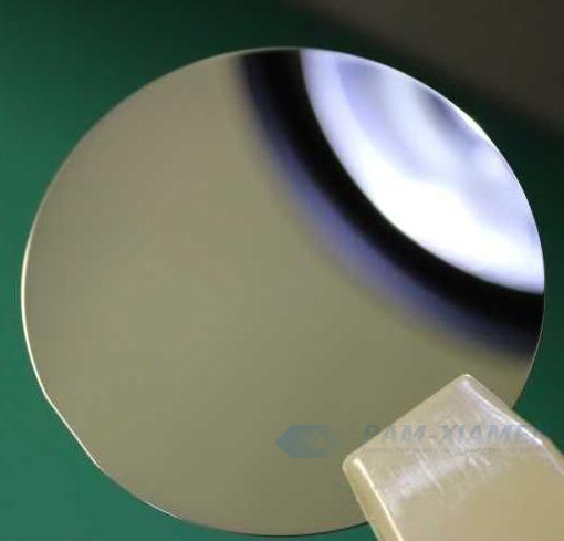
PAM XIAMEN offers 6″ FZ Silicon Ingot with Diameter 150.7±0.3mmØ
Silicon ingot, per SEMI, G 150.7±0.3mmØ
FZ p-type Si:B[110]±2.0°
Ro > 1,000 Ohmcm
Ground Ingot
NO Flats
NOTE: Oxygen<1E16/cc, Carbon<1E16/cc
MCC Lifetime>1,000µs
For more information, send us email at sales@powerwaywafer.com and powerwaymaterial@gmail.com
2020-06-10メタ著者
Metastable rocksalt phase in epitaxial GaN on sapphire
In a series of GaN epilayers grown by metalorganic chemical vapor deposition on sapphire, the GaN rocksalt structure has been detected by x-ray diffraction (XRD) and directly observed by high resolution transmission electron microscopy. The rocksalt GaN [...]
2013-05-07メタ著者
PAM XIAMEN offers 3″ CZ Si Lapped Wafer
3″ CZ Si Lapped Wafer
N-type
Resistivity6-10Ωcm
Thickness180-185um
Orientation <111>
Double Side Lapped
SEMI Flat
For more information, send us email at sales@powerwaywafer.com and powerwaymaterial@gmail.com
2021-01-06メタ著者
Bulk GaN Crystal Grown by HVPE
We succeeded in preparing very thick c-plane bulk gallium nitride (GaN) crystals grown by hydride vapor phase epitaxy. Growth of the bulk GaN crystals was performed on templates with 3 μm GaN layer grown by metal organic chemical vapor [...]
2012-10-16メタ著者
InGaAs nano-pillar array formation on partially masked InP(111)B by selective area metal–organic vapour phase epitaxial growth for two-dimensional photonic crystal application
We report on the selective area metal–organic vapour phase epitaxial growth of an InGaAs nano-pillar array on a partially masked InP(111)B substrate. This technique [...]
2018-04-26メタ著者