PAM-XIAMEN offers 650V GaN FETs chip for fast charge. In current market, gallium nitride fast charging sources mainly use 650V GaN chip (GaN FETs) as power switches, and the high-frequency characteristics of gallium nitride are used to make terminal fast charging products smaller in size and higher [...]
2020-11-24メタ著者
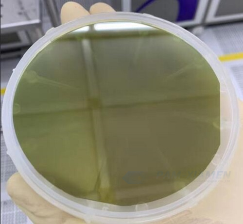
PAM XIAMEN offers test grade silicon wafers
Below is just a short list of the test grade silicon substrates!
Inches
Cust class
Dopant
Type
Orientation
PFL length
PFL direction
SFL
Off orientation
Resistivity
Diameter
Thickness
Bow
TTV
Warp
8
DSP
Phosphorus
N
100
0,0 ± 0,0
110 ± 1
0.0 ± 1.0°
1 – 5 Ohmcm
200 ± 0.5 mm
650 ± 5 µm
20
3
35
8
DSP
Phosphorus
N
100
0,0 ± 0,0
110 ± 1
0.0 ± 0.5°
0.7 – 5.0 [...]
2019-02-25メタ著者
PAM XIAMEN offers 2 inch AlN on sapphire wafer grown by MOCVD, which is the major technology for growing single-crystal aluminum nitride onto large-size, low-cost, and mature sapphire substrate. One important utilization of high-quality AlN-on-sapphire template is the deep ultraviolet (DUV) optoelectronic devices.
1. Specification of [...]
2019-03-11メタ著者
PAM XIAMEN offers 6″FZ Prime Silicon Wafer-1
6″ Si wafer, Diameter 150mm, FZ Gas Dope, SSP, N(100), resistivity 2000-7000Ωcm
PARAMETER
SPECIFICATION
GENERAL CHARACTERISTICS
1
Growth Method
FZ Gas Dope
2
Crystal Orientation
(100)
3
Conductivity Type
n
4
Dopant
Phosphorus
5
Nominal Edge Exclusion
6 mm
ELECTRICAL CHARACTERISTICS
6
Resistivity
2000 – 7000 Ωcm
7
Life Time
>1500 µsec
CHEMICAL CHARACTERISTICS
8
Oxygen Concentrations
< 2xE16 at/cm3
9
Carbon Concentrations
< 2xE16 at/cm3
WAFER PREPARATION CHARACTERISTICS
10
Front Surface Condition
Polished, [...]
2020-04-17メタ著者
PAM-XIAMEN offers (20-2-1) Plane U-GaN Freestanding GaN Substrate
Item
PAM-FS-GAN(20-2-1)-U
Dimension
5 x 10 mm2 or 5 x 20 mm2
Thickness
380+/-50um
Orientation
(20-21)/(20-2-1) plane off angle toward A-axis 0 ±0.5°
(20-21)/(20-2-1) plane off angle toward C-axis -1 ±0.2°
Conduction Type
N-type / Undoped
Resistivity (300K)
< 0.1 Ω·cm
TTV
≤ 10 µm
BOW
BOW ≤ 10 µm
Surface Roughness:
Front side: Ra<0.2nm, epi-ready;
Back side: Fine Ground or polished.
Dislocation Density
≤5 x 106 cm-2
Macro Defect Density
0 cm-2
Useable Area
> 90% (edge exclusion)
Package
each in single wafer container, under nitrogen atmosphere, packed in class 100 clean room
For more information, please contact us email at victorchan@powerwaywafer.com and powerwaymaterial@gmail.com
2020-09-02メタ著者
Silver nanopowder for sale is typically by laser evaporation in vacuum or in a small pressure of gas to get 10 to 100 nm diameters. It can be divided into nano flake silver powder and nano spherical silver powder. Nanomaterials have singular properties that [...]
2021-09-10メタ著者