Semi-insulating indium phosphide (formula: InP) wafer at prime grade for sale is dark gray crystal with a bandwidth (Eg=1.35 eV) at room temperature, a dissociation pressure of 2.75MPa at a melting point, an electron mobility of 4600cm2/(V·s), and a hole mobility of 150cm2/(V·s). PAM-XIAMEN [...]
2021-08-06meta-author
MgO single crystal substrate-1
PAM XIAMEN offers MgO single crystal substrate.
MgO is an excellent single crystal substrate for thin films of Ferro magnetic, Photo-electronic and high Tc superconductor materials. PAM XIAMEN uses a special arc melting method to grow high purity MgO crystal in [...]
2019-05-13meta-author
Graphene and carbon nanotube (CNT) structures have promise for many electronic device applications and both have been grown on SiC through the decomposition of the substrate. It is well known that both graphene and aligned CNTs are grown under similar conditions with overlapping temperature [...]
2019-12-16meta-author
PAM XIAMEN offers 1″ Silicon Wafer.
Material
Orient.
Diam.
Thck
(μm)
Surf.
Resistivity
Ωcm
Comment
n-type Si:P
[100]
1″
475 ±10
E/E
FZ >500 {1,900-2,400}
n-type Si:P
[111] ±0.5°
1″
280
P/P
FZ 2,000-10,000
TTV<5μm
Intrinsic Si:-
[100]
1″
320
P/E
FZ >20,000
Prime
Intrinsic Si:-
[100]
1″
500
P/E
FZ >20,000
SEMI Prime
Intrinsic Si:-
[100]
1″
160
P/P
FZ >10,000
Prime, TTV<8μm
Intrinsic Si:-
[100]
0.5″
12700
C/C
FZ >10,000
a set of 4 rods sealed in polyehtylene foil
Intrinsic Si:-
[111] ±0.5°
1″
500
P/P
FZ >15,000
SEMI Prime
Intrinsic Si:-
[111] ±0.5°
1″
1000
P/E
FZ 14,000-30,000
Cassettes of 7, 6, 6 wafers
Intrinsic Si:-
[111] ±2°
1″
27870
C/C
FZ >10,000
Single Crystal Silicon Rod, 0.39″ diameter × 27.87±0.1mm
p-type [...]
2019-03-08meta-author
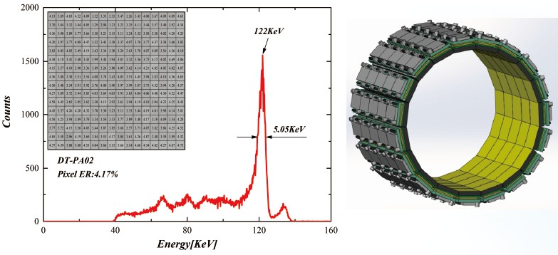
PAM-PA02 is a large size pixel detector based on CZT crystal. They have an extremely high energy resolution and space resolution with a low dose incident of radiation.
1. SPECT, γ-imaging Detector Specification
Material
CdZnTe
Density
5.8g/cm3
Volume resistance
>1010Ω.cm
Dimensions
25.4×25.4mm2
Thickness
5.0mm
Pixel size
1.5×1.5mm2
Pixel pitch
1.6mm
Pixel array
16×16
Electrode material
Au
Operation temperature
+30℃~+40℃
Energy range
20KeV~700MeV
Energy resolution(22℃)
Average<6.5%@122KeV(>13% means defective pixel)
Photo-Peak Efficiency(PPE)
Defined [...]
2019-04-24meta-author
Gallium nitride semiconductors
GaN is a compound semiconductor on steroids! if you could make a 10 Watt part on GaAs at a particular frequency, you can probably make a 100 watt part on GaN right now.
Gallium nitride is the future of microwave power amps, GaAs has exceeded its [...]