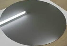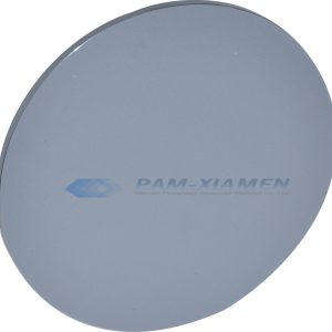
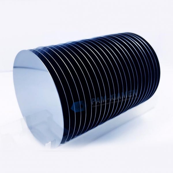
12″ Prime Grade Silicon Wafer
PAM-XIAMEN offer 300mm bare silicon wafers (12 inch) in prime grade, n type or p type, and the 300mm silicon wafer thickness is 775±15. Compared to other silicon wafer suppliers, Powerway Wafer’s silicon wafer price is more competitive with higher quality. 300mm silicon wafers have a higher yield per wafer than pervious large diameter silicon wafers.
- Description
Product Description
PAM-XIAMEN offer 300mm bare silicon wafers (12 inch) in prime grade, n type or p type, and the 300mm silicon wafer thickness is 775±15. Compared to other silicon wafer suppliers, Powerway Wafer’s silicon device wafer price is more competitive with higher quality. 300mm silicon wafers have a higher yield per wafer than pervious large diameter silicon wafers. Size on/above 8 inches (200 mm) is called a large silicon wafer. The production technology of large silicon wafer is not only the increase of process complexity because of the increase of area, but also the higher requirements on many other control factors. For example: oxygen content and its radial uniformity in wafer, impurity control, OISF control, etc. The silicon wafer requirements for defect control, oxygen precipitation control, resistance quantification, doping and radial uniformity are also higher. Especially for prime grade 300mm silicon wafer, some parameters are required critically, for instant, wafer TTV is below1.5um and defect density ~0/cm2. The next step is 450mm silicon ingot or wafer.
1. Parameters of 300mm Silicon Wafer
| Parameters | Value(PAM210512-300-SIL) |
| Type of ingot | Grown according to the Czochralski method |
| Diametr, mm | 300 ± 0,2 |
| Dopant | B (boron) |
| Conductivity type | P |
| Oxigen max, OLD-PPMA | 40 |
| Carbon , PPMA | 1 |
| Crystallographic orientation | <100> |
| Deviation from the predetermined surface orientation of crystal plane, deg | 1 |
| Volume resistivity, Ohm · cm | 8-12 |
| Primary Notch | Yes |
| Notch Location | 110 |
| Notch size, mm | 2,3 |
| Notch Form | V |
| Wafer thickness, microns | 775±15 |
| Type of marking | Laser |
| Marking Location | back side |
| Edge profile | by SEMI T/4 |
| Scratches on the front side | absent |
| Front side polishing | yes |
| Back side polishing | yes |
| Total change in wafer thickness (TTV), micrometers | 1,5 |
| Deflection (WARP), microns | 30 |
| The number of particles on a surface larger than 0.05 microns | 50 |
| The number of particles on a surface larger than 0.09 microns | 30 |
| Surface content of aluminium, E10AT/CM2 | 1 |
| Surface content of calcium, E10AT/CM2 | 1 |
| Surface content of chromium, E10AT/CM2 | 1 |
| Surface content of copper, E10AT/CM2 | 1 |
| Surface content of iron, E10AT/CM2 | 1 |
| Surface content of potassium, E10AT/CM2 | 1 |
| Surface content of natrium, E10AT/CM2 | 1 |
| Surface content of nickel, E10AT/CM2 | 1 |
| Surface content of zinc, E10AT/CM2 | 1 |
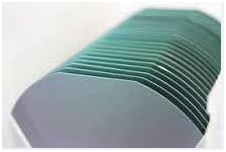
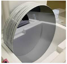
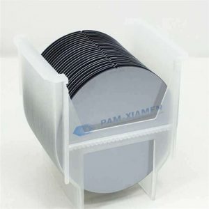
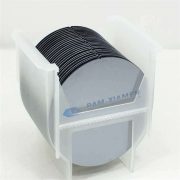
Packing requirements:
| Parameters | |
| Type of packaging | MW300GT-A |
| Inner Container Material | Polyethylene |
| Outer Packing Material | Aluminum |
| Number of pieces in one package | 25 |
| Reusability | Yes |
2. FAQ:
Q: Please take note that we offer “The number of particles on a surface larger than 0.09 microns 50” just for silicon substrate.
Normally the particle requirement is for silicon substrate.
To ensure the compliance, could you please check?
A: We double-checked: Yes, the indicated information is correct.
PAM-XIAMEN can offer you technology and wafer support.
For more information, please visit our website: https://www.powerwaywafer.com/silicon-wafer,
send us email at sales@powerwaywafer.com and powerwaymaterial@gmail.com
Related Products
-
Etching Wafer
The etching silicon wafers offered by PAM-XIAMEN are N type or P type etching wafers, which have low roughness, low reflectivity and high reflectivity. The etching wafer has the characteristics of low roughness, good glossiness and relatively low cost, and directly substitutes the polished wafer or epitaxial wafer which has relatively high cost to produce the electronic elements in some fields, reducing the costs.
-
Epitaxial Silicon Wafer
Silicon Epitaxial Wafer(Epi Wafer) is a layer of epitaxial silicon single crystal deposited onto a single crystal silicon wafer(note: it is available to grow a layer of poly crystalline Silicon layer on top of a highly doped Singly crystalline silicon wafer, but it needs buffer layer (such as oxide or poly-Si) in between the bulk Si substrate and the top epitaxial silicon layer. It also can be used for thin film transistor.
-
Polished Wafer
PAM-XIAMEN can offer polished wafer, n type or p type with orientation at <100>, <110> or <111>. FZ polished wafers, mainly for the production of silicon rectifier (SR), silicon controlled rectifier (SCR), Giant Transistor (GTR), thyristor (GRO)
-
Test Wafer Monitor Wafer Dummy Wafer
As a dummy wafer manufacturer, PAM-XIAMEN offers silicone dummy wafer / test wafer / monitor wafer, which is used in a production device to improve safety in the beginning of production process and are used for delivery check and evaluation of process form. As dummy silicon wafers are often used for experiment and test, size and thickness thereof are important factors in most occasions. 100mm, 150mm, 200mm, or 300mm dummy wafer is available.
-
12″ Test Grade Silicon Wafer
PAM-XIAMEN offers 300mm bare silicon wafers (12 inch) dummy, test grade, n type or p type. Compared to other silicon wafer suppliers, Powerway Wafer offers professional service with competitive prices.
-
Cz Mono-Crystalline Silicon
PAM-XIAMEN, a monocrystalline bulk silicon producer, can offer <100>, <110> and <111> monocrystalline silicon wafers with N&P dopant in 76.2~200 mm, which are grown by CZ method. The Czochralski method is a crystal growth method, referred to as the CZ method. It is integrated in a straight-tube heat system, heated by graphite resistance, melts the polysilicon contained in a high-purity quartz crucible, and then inserts the seed crystal into the surface of the melt for welding. After that, the rotating seed crystal is lowered and melted. The body is infiltrated and touched, gradually raised, and finished or pulled through the steps of necking, necking, shouldering, equal diameter control, and finishing.
-
Float-Zone Mono-Crystalline Silicon
PAM-XIAMEN can offer float zone silicon wafer, which is obtained by Float Zone method. Monocrystalline silicon rods is got through float zone growth, and then process the monocrystalline silicon rods into silicon wafers, called float zone silicon wafers. Since the zone-melted silicon wafer is not in contact with the quartz crucible during the floating zone silicon process, the silicon material is in a suspended state. Thereby, it is less polluted during the process of floating zone melting of silicon. The carbon content and oxygen content are lower, the impurities are less, and the resistivity is higher. It is suitable for the manufacture of power devices and certain high-voltage electronic devices.
-
12″ Silicon Wafers 300mm TOX ( Si Thermal Oxidation Wafer )
PAM-XIAMEN offers 300mm silicon oxide wafer and dioxide wafer. Thermal oxide silicon wafer or silicon dioxide wafer is a bare silicon wafer with oxide layer grown by dry or wet oxidation process. The thermal oxide layer of the silicon wafer is usually grown in a horizontal tube furnace, and the silicon wafer oxide temperature range is generally 900 ℃ ~ 1200 ℃. Compared with CVD oxide layer, silicon wafer oxide layer has higher uniformity, better compactness, higher dielectric strength and better quality.