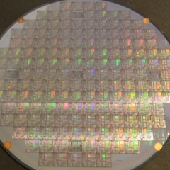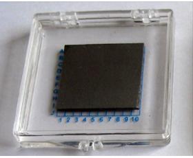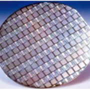
GaAs (Gallium Arsenide) Wafers
As a leading GaAs substrate supplier, PAM-XIAMEN manufactures Epi-ready GaAs(Gallium Arsenide) Wafer Substrate including semi-conducting n type, semi-conductor C doped and p type with prime grade and dummy grade. The GaAs substrate resistivity depends on dopants, Si doped or Zn doped is (0.001~0.009) ohm.cm, C doped one is >=1E7 ohm.cm. The GaAs wafer crystal orientation should be (100) and (111). For (100) orientation, it can be 2°/6°/15° off. The EPD of GaAs wafer normally is <5000/cm2 for LED or <500/cm2 for LD or microelectronics.
- Description
Product Description
(Gallium Arsenide) GaAs Wafer
PAM-XIAMEN develops and manufactures compound semiconductor substrates-gallium arsenide crystal and wafer. We has used advanced crystal growth technology, vertical gradient freeze(VGF) and GaAs wafer manufacturing process, established a production line from crystal growth, cutting, grinding to polishing processing and built a 100-class clean room for GaAs wafer cleaning and packaging. Our GaAs wafers include 2~6 inch ingot/wafers for LED, LD and Microelectronics applications. We are always dedicated to improve the quality of currently GaAs wafer substrates and develop large size substrates. The GaAs wafer size offered is in 2”, 3”, 4” and 6”, and the thickness should be 220-700um. Moreover, the GaAs wafer price from us is competitive.
1. GaAs Wafer Specifications
1.1 (GaAs)Gallium Arsenide Wafers for LED Applications
| Item | Specifications | Remarks |
| Conduction Type | SC/n-type | SC/p-type with Zn dope Available |
| Growth Method | VGF | |
| Dopant | Silicon | Zn available |
| Wafer Diamter | 2, 3 & 4 inch | Ingot or as-cut availalbe |
| Crystal Orientation | (100)2°/6°/15° off (110) | Other misorientation available |
| OF | EJ or US | |
| Carrier Concentration | (0.4~2.5)E18/cm3 | |
| Resistivity at RT | (1.5~9)E-3 Ohm.cm | |
| Mobility | 1500~3000cm2/V.sec | |
| Etch Pit Density | <5000/cm2 | |
| Laser Marking | upon request | |
| Surface Finish | P/E or P/P | |
| Thickness | 220~450um | |
| Epitaxy Ready | Yes | |
| Package | Single wafer container or cassette | |
1.2 (GaAs)Gallium Arsenide Wafers for LD Applications
| Item | Specifications | Remarks |
| Conduction Type | SC/n-type | |
| Growth Method | VGF | |
| Dopant | Silicon | |
| Wafer Diamter | 2, 3 & 4 inch | Ingot or as-cut available |
| Crystal Orientation | (100)2°/6°/15°off (110) | Other misorientation available |
| OF | EJ or US | |
| Carrier Concentration | (0.4~2.5)E18/cm3 | |
| Resistivity at RT | (1.5~9)E-3 Ohm.cm | |
| Mobility | 1500~3000 cm2/V.sec | |
| Etch Pit Density | <500/cm2 | |
| Laser Marking | upon request | |
| Surface Finish | P/E or P/P | |
| Thickness | 220~350um | |
| Epitaxy Ready | Yes | |
| Package | Single wafer container or cassette | |
1.3 (GaAs)Gallium Arsenide Wafers,Semi-insulating for Microelectronics Applications
| Item | Specifications | Remarks |
| Conduction Type | Insulating | |
| Growth Method | VGF | |
| Dopant | C doped | |
| Wafer Diamter | 2, 3 & 4 inch | Ingot available |
| Crystal Orientation | (100)+/- 0.5° | |
| OF | EJ, US or notch | |
| Carrier Concentration | n/a | |
| Resistivity at RT | >1E7 Ohm.cm | |
| Mobility | >5000 cm2/V.sec | |
| Etch Pit Density | <8000 /cm2 | |
| Laser Marking | upon request | |
| Surface Finish | P/P | |
| Thickness | 350~675um | |
| Epitaxy Ready | Yes | |
| Package | Single wafer container or cassette | |
1.4 6″ (150mm)(GaAs)Gallium Arsenide Wafers,Semi-insulating for Microelectronics Applications
| Item | Specifications | Remarks |
| Conduction Type | Semi-insulating | – |
| Grow Method | VGF | – |
| Dopant | C doped | – |
| Type | N | – |
| Diamater(mm) | 150±0.25 | – |
| Orientation | (100)0°±3.0° | – |
| NOTCH Orientation | 〔010〕±2° | – |
| NOTCH Deepth(mm) | (1-1.25)mm 89°-95° | – |
| Carrier Concentration | please consult our sales team | – |
| Resistivity(ohm.cm) | >1.0×10⁷ | – |
| Mobility(cm2/v.s) | please consult our sales team | – |
| Dislocation | please consult our sales team | – |
| Thickness(µm) | 675±25 | – |
| Edge Exclusion for Bow and Warp(mm) | please consult our sales team | – |
| Bow(µm) | please consult our sales team | – |
| Warp(µm) | ≤20.0 | – |
| TTV(µm) | ≤10.0 | – |
| TIR(µm) | ≤10.0 | – |
| LFPD(µm) | please consult our sales team | – |
| Polishing | P/P Epi-Ready | – |
1.5 2″(50.8mm) LT-GaAs (Low Temperature-Grown Galium Arsenide) Wafer Specifications
| Item | Specifications |
| Conduction Type | Semi-insulating |
| Grow Method | VGF |
| Dopant | Sub:C doped / Epi:Undoped |
| Type | N |
| Diamater(mm) | 150±0.25 |
| Orientation | (100)0°±3.0° |
| NOTCH Orientation | 〔010〕±2° |
| NOTCH Deepth(mm) | (1-1.25)mm 89°-95° |
| Carrier Concentration | please consult our sales team |
| Resistivity(ohm.cm) | >1.0×10⁷ or 0.8-9 x10⁻³ |
| Mobility(cm2/v.s) | please consult our sales team |
| Dislocation | please consult our sales team |
| Thickness(µm) | 675±25 |
| Edge Exclusion for Bow and Warp(mm) | please consult our sales team |
| Bow(µm) | please consult our sales team |
| Warp(µm) | ≤20.0 |
| TTV(µm) | ≤10.0 |
| TIR(µm) | ≤10.0 |
| LFPD(µm) | please consult our sales team |
| Polishing | P/P Epi-Ready |
2. GaAs Wafer Market & Application
Gallium arsenide is an important semiconductor material. It belongs to group III-V compound semiconductors and the zinc blende crystal lattice structure, with a lattice constant of 5.65×10⁻¹⁰m, a melting point of 1237°C, and a band gap of 1.4 electron volts. Gallium arsenide can be made into semi-insulating high-resistance materials, which can be used to make integrated circuit substrates, infrared detectors, gamma photon detectors, etc. Because its electron mobility is 5 to 6 times greater than silicon, SI GaAs substrate has been importantly used in the fabrication of microwave devices and high-speed digital circuits. Semiconductor devices fabricated on gallium arsenide have the advantages of high frequency, high temperature, low temperature performance, low noise, and strong radiation resistance, which make the GaAs substrate market enlarge.
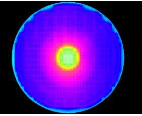
3. Test certificate of GaAs wafer can include below analysis if necessary:
1/Surface roughness of Gallium Arsenide including front side and backside(nanometers).
2/Doping concentration of Gallium Arsenide(cm-3)
3/EPD of Gallium Arsenide(cm-2)
4/Mobility of Gallium Arsendie(V.sec)
5/X-ray diffraction analysis (rocking curves) of Gallium Arsenide: Diffraction reflection curve half-width
6/Low-temperature photoluminescence (emission spectra in the range 0.7-1.0 μm) of Gallium Arsenide: The fraction of exciton photoluminescence in the emission spectrum of the near-IR range at a temperature of 4K or 5 K and an optical excitation density of 1 W / cm2
7/Transmission rate or Absorption coefficient: for instant, we can measure absorption coefficient of single crystal undoped GaAs at 1064nm: <0.6423 cm-1, and this corresponds to a transmission minimum of 33.2% for an exactly 6.5mm thick blank at 1064nm.
Remark:
The Chinese government has announced new limits on the exportation of Gallium materials (such as GaAs, GaN, Ga2O3, GaP, InGaAs, and GaSb) and Germanium materials used to make semiconductor chips. Starting from August 1, 2023, exporting these materials is only allowed if we obtains a license from the Chinese Ministry of Commerce. Hope for your understanding and cooperation!
You may also like…
-
InP wafer
PAM-XIAMEN offers VGF InP(Indium Phosphide) wafer with prime or test grade including low dope, N type or semi-insulating. The mobility of InP wafer is different in different type, low doped one>=3000cm2/V.s, N type>1000 or 2000cm2V.s(depends on different doping concentration), P type: 60+/-10 or 80+/-10cm2/V.s(depends on different Zn doping concentration), and semi-insulting one>2000cm2/V.s, the EPD of Indium Phosphide is below 500/cm2 normally.
-
Ge(Germanium) Single Crystals and Wafers
PAM-XIAMEN offers 2”, 3”, 4” and 6” germanium wafer, which is short for Ge wafer grown by VGF / LEC. Lightly doped P and N type Germanium wafer can be also used for Hall effect experiment. At room temperature, crystalline germanium is brittle and has little plasticity. Germanium has semiconductor properties. High-purity germanium is doped with trivalent elements (such as indium, gallium, boron) to obtain P-type germanium semiconductors; and pentavalent elements (such as antimony, arsenic, and phosphorus) are doped to obtain N-type germanium semiconductors. Germanium has good semiconductor properties, such as high electron mobility and high hole mobility. -
GaAs Epiwafer
PAM-XIAMEN is manufacturing various types of epi wafer III-V silicon doped n-type semiconductor materials based on Ga, Al, In, As and P grown by MBE or MOCVD. We supply custom GaAs epiwafer structures to meet customer specifications, please contact us for more information.
-
Nanofabrication Photoresist
PAM-XIAMEN Offers photoresist plate with photoresist
-
SiC Wafer Substrate
The company has a complete SiC(silicon carbide) wafer substrate production line integrating crystal growth, crystal processing, wafer processing, polishing, cleaning and testing. Nowadays we supply commercial 4H and 6H SiC wafers with semi insulation and conductivity in on-axis or off-axis, available size:5x5mm2,10x10mm2, 2”,3”,4”, 6” and 8″, breaking through key technologies such as defect suppression, seed crystal processing and rapid growth, promoting basic research and development related to silicon carbide epitaxy, devices, etc.
-
CdZnTe (CZT) Wafer
Cadmium Zinc Telluride (CdZnTe or CZT) is a new semiconductor, which enables to convert radiation to electron effectively, it is mainly used in infrared thin-film epitaxy substrate, X-ray detectors and Gamma-ray CdZnTe detectors. -
Freestanding GaN substrate
PAM-XIAMEN has established the manufacturing technology for freestanding (gallium nitride)GaN substrate wafer, which is for UHB-LED and LD. Grown by hydride vapour phase epitaxy (HVPE) technology,Our GaN substrate has low defect density.
-
Float-Zone Mono-Crystalline Silicon
PAM-XIAMEN can offer float zone silicon wafer, which is obtained by Float Zone method. Monocrystalline silicon rods is got through float zone growth, and then process the monocrystalline silicon rods into silicon wafers, called float zone silicon wafers. Since the zone-melted silicon wafer is not in contact with the quartz crucible during the floating zone silicon process, the silicon material is in a suspended state. Thereby, it is less polluted during the process of floating zone melting of silicon. The carbon content and oxygen content are lower, the impurities are less, and the resistivity is higher. It is suitable for the manufacture of power devices and certain high-voltage electronic devices.