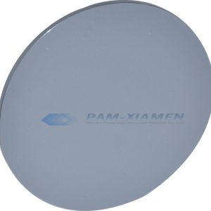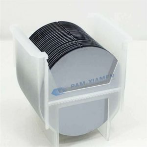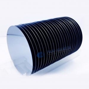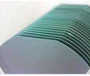
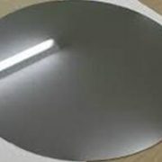
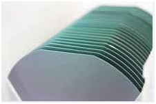
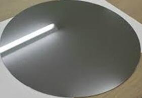
Polished Wafer
PAM-XIAMEN can offer polished wafer, n type or p type with orientation at <100>, <110> or <111>. FZ polished wafers, mainly for the production of silicon rectifier (SR), silicon controlled rectifier (SCR), Giant Transistor (GTR), thyristor (GRO)
- Description
Product Description
Polished wafer
PAM-XIAMEN can offer polished wafer, n type or p type with orientation at <100>, <110> or <111>. More Specifications, please see tables below.
Our advantages at a glance
- Advanced epitaxy growth equipment and test equipment.
- Offer the highest quality with low defect density and good surface roughness.
- Strong research team support and technology support for our customers
1. Specifications of Polished Silicon Wafers
1.1 FZ Polished Wafers Specifications
FZ polished silicon wafer: mainly for the production of silicon rectifier (SR), silicon controlled rectifier (SCR), Giant Transistor (GTR), thyristor (GRO)
| Type | Conduction type | Orientation | Diameter scope(mm) | Resistivity scope(Ω cm) | Geometric parameter graininess,surface metal |
| FZ | N&P | <100>&<111> | 76.2-200 | >1000 | T≥260(um) TTV≤2(um) TIR≤2(um) STIR≤1(um)(20*20) Graininess≤10pcs(≥0.3um) , ≤20pcs(≥ urface metal≤5E10/cm2 BSD:Etchpit density>1E106pcs/cm2 Poly:5000-12000 A |
| NTDFZ | N | <100>&<111> | 76.2-200 | 30-800 | |
| CFZ | N&P | <100>&<111> | 76.2-200 | 1-50 | |
| GDFZ | N&P | <100>&<111> | 76.2-200 | 0.001-300 |
1.2 CZ Polished Wafers Specifications
| Type | Conduction type | Orientation | Diameter scope(mm) | Resistivity scope(Ω cm) | Geometric parameter graininess,surface metal |
| MCZ | N&P | <100> <110>&<111> | 76.2-200 | 1-300 | T≥260(um) TTV≤2(um) TIR≤2(um) STIR≤1(um)(20*20) Graininess≤10pcs(≥0.3um) ,≤20pcs(≥0.2um) Surface metal≤5E10/cm2 BSD:Etchpit density>1E106pcs/cm2LTO:3500~8000±250A |
| CZ | N&P | <100> <110>&<111> | 76.2-200 | 1-300 | |
| MCZ heavily doped | N&P | <100>&<111> | 76.2-200 | 0.001-1 |
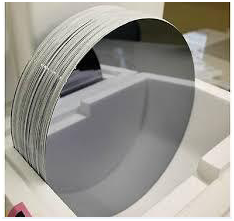
2. About Polished Wafer
High-purity electronic grade polysilicon undergoes the steps of crystal pulling, slicing, beveling, lapping, etching, polishing, and cleaning to produce a polished wafer, which meets electrical, surface physical properties, impurity standards and other specifications. Wafers with special processes such as annealing, epitaxy, and SOI are processed based on polished wafers.
Polished wafer (PW) is a silicon chip with atomic flatness that is single side or double sides polished silicon wafer, accounting for about 70% of silicon wafer applications. After the monocrystalline silicon ingot is produced, it is cut into thin slices from the cylindrical monocrystalline silicon of the ingot, which is a wafer of high-purity silicon element. The purpose of polishing is to further remove the residual damage layer on the processed surface. The polished monocrystalline silicon wafer can be directly used to fabricate devices or as an epitaxial substrate material. Polished Si wafer is widely used in digital and analog integrated circuits, memory, power devices and other chips.
N Type Sb Doped Silicon Wafer for Integrated Circuit Manufacturing
PAM XIAMEN offers MCZ silicon ingot and silicon wafer.
PAM XIAMEN offers black lithium Niobate wafers for optics and SAW Components
Stoichiometric LPCVD Nitride on Silicon Wafers
4″ Prime CZ Si wafer with one side sputtering Cr/Au layer thickness 10/50nm
Zero Diffraction Si Wafer Diameter 32mm for XRD measurements
Silicon Nitride Waveguide – Substrates and Services Provided
Super Low Stress Nitron on Silicon Wafers
Low Stress Nitride Silicon Wafers
Silicon Wafers with (211) Orientation
Silicon Wafers for Soft Lithography
Silicon Wafers PDMS Micro-Fluidic Chip Platforms
Silicon Wafer Thickness:275+- 25µm
Silicon Wafer Thickness:1000μm
2″ silicon wafers Thickness:1000 ±25μm
Si wafer Thickness: 675 ± 25 um
4″ Si wafer Thickness:500±20μm
3″ Si wafer Thickness: 380±20μm
50.8mm (2 Inch) Silicon Wafers-1
50.8mm (2 Inch) Silicon Wafers-2
50.8mm (2 Inch) Silicon Wafers-3
50.8mm (2 Inch) Silicon Wafers-4
50.8mm (2 Inch) Silicon Wafers-5
76.2mm (3 Inch) Silicon Wafers
100mm (4 Inch) Silicon Wafers-1
100mm (4 Inch) Silicon Wafers-2
100mm (4 Inch) Silicon Wafers-3
100mm (4 Inch) Silicon Wafers-4
100mm (4 Inch) Silicon Wafers-5
100mm (4 Inch) Silicon Wafers-6
(100) Oriented Silicon Wafers-1
(100) Oriented Silicon Wafers-2
(100) Oriented Silicon Wafers-3
(100) Oriented Silicon Wafers-4
(100) Oriented Silicon Wafers-5
(112) Orientation Silicon Wafers
4″ FZ Intrinsic Silicon Wafer SSP
You may also like…
-
Float-Zone Mono-Crystalline Silicon
PAM-XIAMEN can offer float zone silicon wafer, which is obtained by Float Zone method. Monocrystalline silicon rods is got through float zone growth, and then process the monocrystalline silicon rods into silicon wafers, called float zone silicon wafers. Since the zone-melted silicon wafer is not in contact with the quartz crucible during the floating zone silicon process, the silicon material is in a suspended state. Thereby, it is less polluted during the process of floating zone melting of silicon. The carbon content and oxygen content are lower, the impurities are less, and the resistivity is higher. It is suitable for the manufacture of power devices and certain high-voltage electronic devices.
-
GaAs (Gallium Arsenide) Wafers
As a leading GaAs substrate supplier, PAM-XIAMEN manufactures Epi-ready GaAs(Gallium Arsenide) Wafer Substrate including semi-conducting n type, semi-conductor C doped and p type with prime grade and dummy grade. The GaAs substrate resistivity depends on dopants, Si doped or Zn doped is (0.001~0.009) ohm.cm, C doped one is >=1E7 ohm.cm. The GaAs wafer crystal orientation should be (100) and (111). For (100) orientation, it can be 2°/6°/15° off. The EPD of GaAs wafer normally is <5000/cm2 for LED or <500/cm2 for LD or microelectronics.
-
SiC Wafer Substrate
The company has a complete SiC(silicon carbide) wafer substrate production line integrating crystal growth, crystal processing, wafer processing, polishing, cleaning and testing. Nowadays we supply commercial 4H and 6H SiC wafers with semi insulation and conductivity in on-axis or off-axis, available size:5x5mm2,10x10mm2, 2”,3”,4”, 6” and 8″, breaking through key technologies such as defect suppression, seed crystal processing and rapid growth, promoting basic research and development related to silicon carbide epitaxy, devices, etc.
-
Epitaxial Silicon Wafer
Silicon Epitaxial Wafer(Epi Wafer) is a layer of epitaxial silicon single crystal deposited onto a single crystal silicon wafer(note: it is available to grow a layer of poly crystalline Silicon layer on top of a highly doped Singly crystalline silicon wafer, but it needs buffer layer (such as oxide or poly-Si) in between the bulk Si substrate and the top epitaxial silicon layer. It also can be used for thin film transistor.
-
Etching Wafer
The etching silicon wafers offered by PAM-XIAMEN are N type or P type etching wafers, which have low roughness, low reflectivity and high reflectivity. The etching wafer has the characteristics of low roughness, good glossiness and relatively low cost, and directly substitutes the polished wafer or epitaxial wafer which has relatively high cost to produce the electronic elements in some fields, reducing the costs.
-
Cz Mono-Crystalline Silicon
PAM-XIAMEN, a monocrystalline bulk silicon producer, can offer <100>, <110> and <111> monocrystalline silicon wafers with N&P dopant in 76.2~200 mm, which are grown by CZ method. The Czochralski method is a crystal growth method, referred to as the CZ method. It is integrated in a straight-tube heat system, heated by graphite resistance, melts the polysilicon contained in a high-purity quartz crucible, and then inserts the seed crystal into the surface of the melt for welding. After that, the rotating seed crystal is lowered and melted. The body is infiltrated and touched, gradually raised, and finished or pulled through the steps of necking, necking, shouldering, equal diameter control, and finishing.
-
Test Wafer Monitor Wafer Dummy Wafer
As a dummy wafer manufacturer, PAM-XIAMEN offers silicone dummy wafer / test wafer / monitor wafer, which is used in a production device to improve safety in the beginning of production process and are used for delivery check and evaluation of process form. As dummy silicon wafers are often used for experiment and test, size and thickness thereof are important factors in most occasions. 100mm, 150mm, 200mm, or 300mm dummy wafer is available.
-
Freestanding GaN substrate
PAM-XIAMEN has established the manufacturing technology for freestanding (gallium nitride)GaN substrate wafer, which is for UHB-LED and LD. Grown by hydride vapour phase epitaxy (HVPE) technology,Our GaN substrate has low defect density.


Related Products
-
12″ Silicon Wafers 300mm TOX ( Si Thermal Oxidation Wafer )
PAM-XIAMEN offers 300mm silicon oxide wafer and dioxide wafer. Thermal oxide silicon wafer or silicon dioxide wafer is a bare silicon wafer with oxide layer grown by dry or wet oxidation process. The thermal oxide layer of the silicon wafer is usually grown in a horizontal tube furnace, and the silicon wafer oxide temperature range is generally 900 ℃ ~ 1200 ℃. Compared with CVD oxide layer, silicon wafer oxide layer has higher uniformity, better compactness, higher dielectric strength and better quality.
-
12″ Test Grade Silicon Wafer
PAM-XIAMEN offers 300mm bare silicon wafers (12 inch) dummy, test grade, n type or p type. Compared to other silicon wafer suppliers, Powerway Wafer offers professional service with competitive prices.
-
12″ Prime Grade Silicon Wafer
PAM-XIAMEN offer 300mm bare silicon wafers (12 inch) in prime grade, n type or p type, and the 300mm silicon wafer thickness is 775±15. Compared to other silicon wafer suppliers, Powerway Wafer’s silicon wafer price is more competitive with higher quality. 300mm silicon wafers have a higher yield per wafer than pervious large diameter silicon wafers.