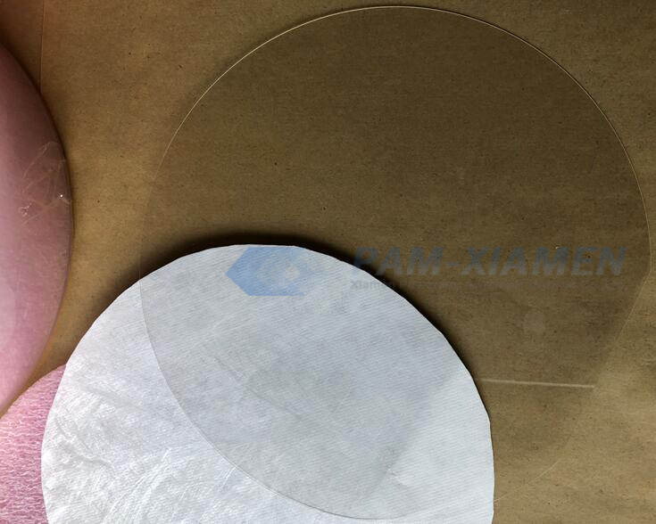
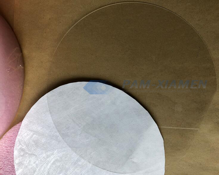
We are one of the world’s leading glass wafer suppliers, provide thin & ultra-thin glass wafers and substrates which are made of different materials, such as Borofloat, Fused Silica & Quartz, BK7, Soda Lime etc for MEMS, fiber optic AWG、 LCDパネル と OLED基板 application. These wafers are all SEMI Standards including dimensional, flat and notch specifications, also we offer custom specifications designed to your unique needs including alignment marks, holes, pockets, edge profile, thickness, flatness, surface quality, cleanliness or any other details critical to your application, including semiconductor, medical science, communications, lasers, infrared, electronics, measuring instruments, military, and aerospace.
1. Specification of Glass Wafer
| パラメーター | 測定 |
| 直径 | 2 "、4"、6 "、8"、10 " |
| 寸法公差 | ±0.02μmで |
| 厚さ | 0.12ミリメートル、0.13ミリメートル、0.2ミリメートル、0.25ミリメートル、0.45ミリメートル |
| 厚さ公差 | ±10μmで |
| 厚さ変動(TTV) | <0.01ミリメートル |
| 扁平 | 1/10ウェーブ/インチ |
| 表面粗さ(RMS) | <1.5nm |
| スクラッチと掘ります | May 2nd |
| 粒子サイズ | <5μmの |
| ボウ/ワープ | <10μM |
| カスタマイズされたディメンションの場合は、お問い合わせください | |
2. Glass Wafer Process
Wafer Cutting: blank wafer are ready through that thick sheets are water jetted and blocks are wire sawn
Ground Edge: the wafer edge is cylindrical grounded on the Edge Grinding Station.
Wafer Lapping: the wafer is lapped to appointed thickness.
Wafer Polishing: Polishing the wafer gives it the mirrored, super-flat surface required for the fabrication.
Wafer Cleaning: it is the removal of chemical and particle impurities without altering or damaging the wafer surface or substrate on multiple cleaning lines.
Wafer Inspection: inspect to various quality levels under the appropriate lighting condition in the Class 100 Clean Room.
Wafer Packaging: All wafers are packed in the single wafer containers.
3. Transmittance of Glass Wafer
ガラスウェーハ
Transmittance of Glass Wafer
4. Scratch/Dig Inspection Standard for Glass Wafer
We inspect the glasses for scratches by strong light (Multi-angle parallel light source) in a dark room.
Inspection Purpose: To determine whether there are fine scratches, foreign bodies, microbubbles on the glass surface.
Inspection Content: Inspect for fine scratch on glass surface
Reference Light Source: Multi-angle parallel light source
Analysis: The inspection for fine scratch, foreign matter on glass surface.
The glass is a highly reflective object, and the multi-angle parallel light source can illuminate the fine scratches clearly, and very uniform.
Scratch/Dig: 60/40 means:
60: max allowable scratch width (0.06mm width)
40: max allowable dig diameter (0.4mm diameter)
More about the scratch or dig number, please refer to the table below:
| Scratch Number | Maximum Allowable Scratch Width (mm) |
Dig Number | Maximum Allowable Dig or Bubble Diameter (mm) |
|
| 120 | 0.12 | 120 | 1.2 | |
| 80 | 0.08 | 80 | 0.8 | |
| 60 | 0.06 | 60 | 0.6 | |
| 50 | 0.05 | 50 | 0.5 | |
| 40 | 0.04 | 40 | 0.4 | |
| 30 | 0.03 | 30 | 0.3 | |
| 20 | 0.02 | 20 | 0.2 | |
| Purpose: glass surface quality on optical components Definitions: Procedure: |
||||
詳細については、メールでお問い合わせください。victorchan@powerwaywafer.com と powerwaymaterial@gmail.com.