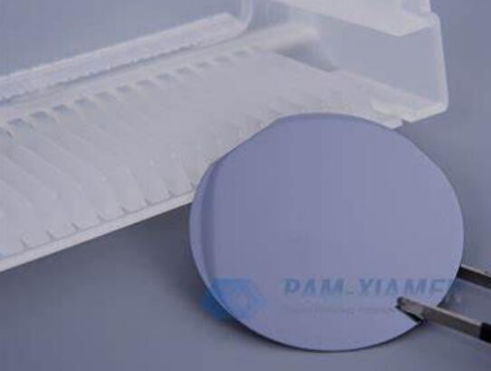
ダミーグレードの単結晶リン化インジウムウェーハは、VGFによって成長したドーピングSで利用できます。 N型リン化インジウムウェーハの電子濃度が10に達する18cm-3、およびリン化インジウムの抵抗率は非常に低く、一般に10-2~10-3Ω·cm. It is mostly used in high-speed optoelectronic devices, such as LD, LED, PIN- PD, PIN-APD and etc. EPD map of InP can be offered if necessary, please contact us at victorchan@powerwaywafer.com. The specifications of the test grade InP wafers 次のようにリストされています。
1.ダミーグレードのリン化インジウムウェーハの仕様
項目1:
| アイテム | パラメーター | 単位 |
| 材料 | リン化インジウムウェーハ | |
| グレード | ダミーグレード | |
| 直径 | 50.0±0.5 | ミリ |
| 厚さ | 最小:300最大:400 | ええと |
| 方向付け | (100)±0.5° | |
| 導電率タイプ/ドーパント | SCN / S | |
| プライマリフラット長 | 16±2 | ミリ |
| プライマリオリエンテーションフラット | EJ(0-1-1) | |
| セカンダリフラット長 | 7±1 | ミリ |
| 二次オリエンテーションフラット | EJ(0-11) | |
| キャリア濃度 | 最小:/最大:/ | cm-3 |
| 抵抗率 | 最小:/最大:/ | オームセンチメートル |
| モビリティ | 最小:/最大:/ | cm2/ V * Sec |
| EPD | アベニュー:/最大:<1000 cm-2 | cm-2 |
| TTV | 10 | ええと |
| TIR | 10 | ええと |
| 弓 | 10 | ええと |
| ワープ | 15 | ええと |
| 表面 | P / P、P / E | |
| エッジの丸め | 0.25(SEMI規格に準拠) | mmR |
| エピレディ | はい | |
| レーザマーク | / | |
| ラメラツインエリア | (100)配向> 80%の有用な単結晶領域 | |
| パッケージ | Nで満たされた個々のコンテナ2 |
項目2:
| アイテム | パラメーター | 単位 |
| 材料 | リン化インジウム基質 | |
| グレード | ダミーグレード | |
| 直径 | 76.2±0.5 | ミリ |
| 厚さ | 最小:600最大:650 | ええと |
| 方向付け | (100)±0.5° | |
| 導電率タイプ/ドーパント | SCN / S | |
| プライマリフラット長 | 22±1 | ミリ |
| プライマリオリエンテーションフラット | EJ | |
| セカンダリフラット長 | 12±1 | ミリ |
| 二次オリエンテーションフラット | EJ | |
| キャリア濃度 | 最小:/最大:/ | cm-3 |
| 抵抗率 | 最小:/最大:/ | オームセンチメートル |
| モビリティ | 最小:/最大:/ | cm2/ V * Sec |
| EPD | アベニュー:/最大:<1000 cm-2 | cm-2 |
| TTV | 10 | ええと |
| TIR | 10 | ええと |
| 弓 | 10 | ええと |
| ワープ | 15 | ええと |
| 表面 | P / P、P / E | |
| エッジの丸め | 0.25(SEMI規格に準拠) | mmR |
| エピレディ | はい | |
| レーザマーク | / | |
| ラメラツインエリア | (100)配向> 80%の有用な単結晶領域 | |
| パッケージ | Nで満たされた個々のコンテナ2 |
項目3:
| アイテム | パラメーター | 単位 |
| 材料 | リン化インジウムウェーハ | |
| グレード | ダミーグレード | |
| 直径 | 100.0±0.5 | ミリ |
| 厚さ | 最小:600最大:650 | ええと |
| 方向付け | (100)±0.5° | |
| 導電率タイプ/ドーパント | SCN / S | |
| プライマリフラット長 | 32.5±1 | ミリ |
| プライマリオリエンテーションフラット | EJ | |
| セカンダリフラット長 | 18±1 | ミリ |
| 二次オリエンテーションフラット | EJ | |
| キャリア濃度 | 最小:/最大:/ | cm-3 |
| 抵抗率 | 最小:/最大:/ | オームセンチメートル |
| モビリティ | 最小:/最大:/ | cm2/ V * Sec |
| EPD | アベニュー:/最大:<1000 cm-2 | cm-2 |
| TTV | 10 | ええと |
| TIR | 10 | ええと |
| 弓 | 10 | ええと |
| ワープ | 15 | ええと |
| 表面 | P / P、P / E | |
| エッジの丸め | 0.25(SEMI規格に準拠) | mmR |
| エピレディ | はい | |
| レーザマーク | / | |
| ラメラツインエリア | (100)配向> 80%の有用な単結晶領域 | |
| パッケージ | Nで満たされた個々のコンテナ2 |
2.ダミーグレードのリン化インジウムアプリケーション
ダミーグレードのInPウェーハは、エピタキシャル層のエピ成長プロセステストと組成特性評価に使用されます。 ツイン結晶とツイン側のウェーハ配向の穴の可能性があるため、導波路や光学格子などのデバイス構造のエッチングには適していません。
マイクロツインまたはウェーハ表面の系統<20%が許容されます。
3.リン化インジウムの特性
Indium phosphide is a group III-V compound semiconductor material compounded by the combination of group III element indium (In) and group V element phosphorus (P). It has a zinc blende structure with a indium phosphide lattice constant of 0.586 9 nm. InP single crystal is soft and brittle, silver-gray with metallic luster. The indium phosphide band gap at room temperature is 1.344 eV, which is a direct transition band structure. The emission wavelength is 0.92 um, the intrinsic carrier concentration of InP at room temperature is 2×10⁷CM-3、および電子と正孔の移動度は4 500 cm2/ Vsと150cm2 / V・sそれぞれ。

リン化インジウムの結晶構造
4.InPウェーハ製造プロセス
リン化インジウムは、ガリウム砒素GaAsおよびほとんどのIII-V半導体とほぼ同じ面心立方結晶構造を持っています。 リン化インジウムウェーハは、デバイスの製造前に準備する必要があり、スライス中の表面の損傷を排除するために重ね合わせる必要があります。 InPのダミーウェーハは、最終的な材料除去段階で化学機械研磨(CMP)され、原子スケールの超平坦な粗さの鏡面を実現します。
However, the growth process of indium phosphide from raw materials to ingots to wafers is very difficult. During the growth process, a high temperature of 1070℃ and extreme pressure are required. In addition, the atomic structure may change. What comes out may not meet expectations. From raw materials to ingots to a 2-inch or 4-inch indium phosphide single crystal wafer, the yield is generally about 28%, and the technical threshold is very high. Therefore, PAM-XIAMEN is one of the indium phosphide wafer suppliers that can successfully control the growth technology of indium phosphide. Relying on VGF, VB method crystal growth technology, high surface quality wire cutting technology, ultra-flat mechanical chemical polishing technology, ultra-clean surface cleaning technology and other related core technologies, the commercialization of indium phosphide wafers tends to be stable, and the products provided by PAM-XIAMEN are mainly used in optical fiber communications, optical detectors, infrared optics, high-frequency millimeter wave communications and other fields. In addition to the current application areas, the monocrystalline indium phosphide wafer substrate will expand in the terahertz field used in 6G communications.
5.InP材料の将来の開発
In fact, InP substrate material is the most critical core material in the optical communication industry chain, ultra-high frequency millimeter wave radar, infrared detection and other fields. It is inseparable from indium phosphide since the demand for higher bandwidth continues to grow, especially in the Human-driven cars, 5G communications, even the implementation and application of 6G, 7G, and 8G in the future. The indium phosphide wafer market at dummy or prime grade will usher in rapid growth, thereby, the indium phosphide wafer cost will go down.

詳細については、メールでお問い合わせください。 victorchan@powerwaywafer.com と powerwaymaterial@gmail.com.