PAM XIAMEN offers 4″CZ Epitaxial Prime Silicon Wafer.
4″ Si epi wafer
Growth Method: CZ
100 +/- 0.5 mm diameter silicon
Orientation <111> 4deg off
P Type Boron doped 0.002 – 0.003 ohm cm
Front side polished – Epi ready
thickness 525 +/-25 um [...]
2019-07-05meta-author
PAM XIAMEN offers 4″ Silicon Wafer.
Material
Orient.
Diam.
Thck
(μm)
Surf.
Resistivity
Ωcm
Comment
n-type Si:Sb
[211] ±0.5°
4″
1,500 ±15
P/P
0.01-0.02
SEMI Prime, TTV<1μm
n-type Si:Sb
[211] ±0.5°
4″
1600
C/C
0.01-0.02
SEMI Test, Wafers can be polished for additional fee
n-type Si:P
[111]
4″
1200
P/P
35-85
SEMI Prime
n-type Si:P
[111] ±0.5°
4″
1500
P/E
>20 {24-29}
SEMI Prime, TTV<5μm, in Empak cassettes of 2 wafers
n-type Si:P
[111] ±0.5°
4″
250
P/E
18-25
SEMI Prime
n-type Si:P
[111] ±0.5°
4″
500
P/P
11-15
SEMI Prime, Both-sides Epi Ready polished
n-type Si:P
[111]
4″
280
P/E
1.3-2.7
SEMI Prime
n-type Si:P
[111] ±0.5°
4″
280
P/E
1.3-2.7
SEMI Prime
n-type [...]
2019-03-05meta-author
Highlights
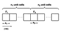
•A recessed structure was used on the GaAs/Si solar cells to reduce the current path.
•The associated series resistance was reduced by a recessed structure.
•The carrier recombination loss was improved due to pyramid-like recessed structure.
In this study, epitaxial layers of GaAs-based solar cells were grown [...]
III-nitrides are mainly composed of InN-GaN-AlN and its alloys, of which InGaN is the most important and widely used. InGaN is unstable and easy to decompose at high temperature. The separated phase InN can form small clusters with three-dimensional quantum confinement, which strengthens the [...]
2023-02-16meta-author
PAM XIAMEN offers Zinc Oxide on Silicon.
The following wafers work
Thermal oxide Layer
Research Grade , about 80 % useful area
SiO2 layer on 4″ Silicon wafer
Dry Oxide layer thickness: 100 nm ( 2000A) +/-10%
Growth method – Dry oxidizing at 1000oC
Refractive index – 1.455
Note: customized oxide layer [...]
2019-02-26meta-author
PAM XIAMEN offers 4″ Silicon EPI Wafers.
Substrate
EPI
Comment
Size
Type
Res
Ωcm
Surf.
Thick
μm
Type
Res
Ωcm
4″Øx400μm
n- Si:As[111]
0.001-0.005
P/E
21
n- Si:P
0.15
n/n+
4″Øx360μm
n- Si:Sb[111]
0.005-0.020
P/E
20
n- Si:P
360 – 440
n/n+
4″Øx400μm
p- Si:B[111]
0.01-0.10
P/E
6.5
p- Si:B
3.6±10%
P/P/P+
4″Øx400μm
p- Si:B[111]
0.01-0.10
P/E
22±1.5
p- Si:B
300±50
P/P/P+
4″Øx525μm
p- Si:B[111]
0.01-0.02
P/E
8.1±1
p- Si:B
4.5±10%
P/P/P+
4″Øx525μm
p- Si:B[111]
0.01-0.02
P/E
6.85±0.75
p- Si:B
0.75±0.15
P/P/P+
4″Øx380μm
p- Si:B[111]
0.008-0.020
P/EOx
10.5
p- Si:B
570±10%
p/p+
4″Øx440μm
p- Si:B[111]
0.008-0.020
P/E
20
p- Si:B
0.25±10%
P/P+
4″Øx525μm
p- Si:B[111]
0.001-0.005
P/E
20
p- Si:B
175±10%
P/P+
4″Øx440μm
p- Si:B[111]
0.008-0.020
P/E
21
p- Si:B
150 ±10%
P/P+
4″Øx380μm
p- Si:B[111]
0.008-0.020
P/EOx
23
p- Si:B
80±10%
P/P+
4″Øx380μm
p- Si:B[111]
0.008-0.020
P/EOx
23
p- Si:B
200±10%
P/P+
4″Øx440μm
p- Si:B[111]
0.008-0.020
P/E
32
p- Si:B
600 ±10%
P/P+
4″Øx440μm
p- Si:B[111]
0.01-0.02
P/E
32.5
p- Si:B
100±10%
P/P+
4″Øx380μm
p- Si:B[111]
0.008-0.020
P/EOx
40
p- Si:B
550 ±10%
P/P+
4″Øx525μm
n- Si:As[111]
0.0010-0.0035
P/E
20
p- Si:B
10±1.5
P/N/N+
4″Øx525μm
n- [...]
2019-03-08meta-author