III-nitrides are mainly composed of InN-GaN-AlN and its alloys, of which InGaN is the most important and widely used. InGaN is unstable and easy to decompose at high temperature. The separated phase InN can form small clusters with three-dimensional quantum confinement, which strengthens the carrier confinement and improves the recombination efficiency, which is very beneficial to luminescence. InGaN / GaN heterojunction quantum wells are the core structure of high-performance light sources and new high-frequency transistor devices, which play a key role in the quantum limitation and high-speed transmission of carriers. PAM-XIAMEN can offer wafers with InGaN/GaN multiple quantum well, for more information please visit https://www.powerwaywafer.com/gan-wafer. Moreover, we can provide sapphire based InGaN / GaN heteroepitaxial services for your academic research studies, like characterizing nitride heterostructures. Just take the following epitaxial structure of InGaN / GaN heterojunction as an example:
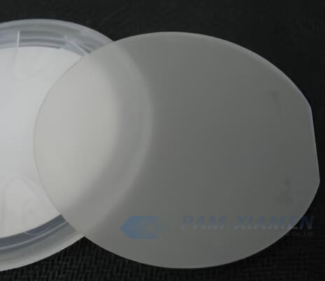
1. 2inch InGaN / GaN Heterostructure on Sapphire
PAMP20013 – INGANE
| Layer No. | Material | Thickness |
| 4 | Undoped GaN | – |
| 3 | InGaN (30% In) | 2nm |
| 2 | Undoped GaN | – |
| 1 | Insulating GaN | – |
| 0 | Sapphire Substrate |
Please kindly note:
- The In of InGaN componentis 30%+/-5%, because the thickness is only 2nm, too thin, very difficult to control;
- If you need to use optical spectroscopies in your studies, thick GaN is suggested to avoid Fabri-Perot interference of the light.
- The InGaN layer is not intentionally doped. Because there is a thin layer of high in component InGaN under IGaN, in order to prevent in evaporation during high temperature process, the growth temperature of I-GaN layer is lower (the same as InGaN growth temperature). Therefore, we think that low temperature growth introduces more C, resulting in high resistance of I-GaN. Therefore, it is inevitable that contact can not be done.
- If you need a contact structure process for InGaN / GaN structure in the future, we will adopt another special intermediate treatment layer to meet the requirements of epitaxial structure and contact technology at the same time. If any inquiries, please contact our sales team at victorchan@powerwaywafer.com.
2. Influencing Factors for Luminous Characteristics of Devices on InGaN / GaN Structure
The active region of InGaN/GaN structure is a key component of light-emitting devices. The light-emitting characteristics of devices are mainly affected by two mechanisms:
- Due to the fluctuation of In component (quantity concentration of matter), the In-rich clusters or quantum dots are formed, resulting in the localization of carriers. The energy level filling effect of the local state will affect the luminous efficiency and the luminous peak of the device.
- For GaN light-emitting devices with the c-plane (0001) as the growth surface and its normal direction (c-axis) as the growth direction, due to the difference in theInGaN GaN lattice constant, the InGaN active layer is subject to stress, which will cause a large piezoelectric polarization field inside the material, resulting in the tilt of the energy band in QW and the reduction of the overlap of the electron hole wave functions.
Remark:
The Chinese government has announced new limits on the exportation of Gallium materials (such as GaAs, GaN, Ga2O3, GaP, InGaAs, and GaSb) and Germanium materials used to make semiconductor chips. Starting from August 1, 2023, exporting these materials is only allowed if we obtains a license from the Chinese Ministry of Commerce. Hope for your understanding and cooperation!

For more information, please contact us email at victorchan@powerwaywafer.com and powerwaymaterial@gmail.com.