Product Specifications
PAM XIAMEN offers Freestanding GaN Substrate
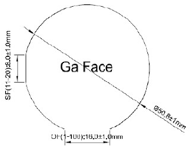
2″GaN Free-standing Substrate
| Item | PAM-FS-GaN50-N | PAM-FS-GaN50-SI |
| Conduction Type | N-type | Semi-insulating |
| Size | 2″(50.8)+/-1mm | |
| Thickness | 260+/-20um | |
| Orientation | C-axis(0001)+/-0.5° | |
| Primary Flat Location | (1-100)+/-0.5° | |
| Primary Flat Length | 16+/-1mm | |
| Secondary Flat Location | (11-20)+/-3° | |
| Secondary Flat Length | 8+/-1mm | |
| Resistivity(300K) | <0.5Ω·cm | >10^6Ω·cm |
| Dislocation Density | <5×10^6cm-2 | |
| Marco Defect Density | A grade<=2cm-2 B grade>2cm-2 | |
| TTV | <=15um | |
| BOW | <=20um | |
| Surface Finish | Front Surface:Ra<0.2nm.Epi-ready polished Back Surface:1.Fine ground 2.Rough grinded ≥ 90 % |
|
Usable Area
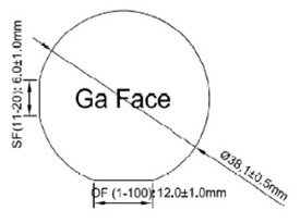
1.5″GaN Free-standing Substrate
| Item | PAM-FS-GaN50-N | PAM-FS-GaN50-SI |
| Conduction Type | N-type | Semi-insulating |
| Size | 1.5″(38.1)+/-0.5mm | |
| Thickness | 260+/-20um | |
| Orientation | C-axis(0001)+/-0.5° | |
| Primary Flat Location | (1-100)+/-0.5° | |
| Primary Flat Length | 12+/-1mm | |
| Secondary Flat Location | (11-20)+/-3° | |
| Secondary Flat Length | 6+/-1mm | |
| Resistivity(300K) | <0.5Ω·cm | >10^6Ω·cm |
| Dislocation Density | <5×10^6cm-2 | |
| Marco Defect Density | A grade<=2cm-2 B grade>2cm-2 | |
| TTV | <=15um | |
| BOW | <=20um | |
| Surface Finish | Front Surface:Ra<0.2nm.Epi-ready polished Back Surface:1.Fine ground 2.Rough grinded ≥ 90 % |
|
Usable Area
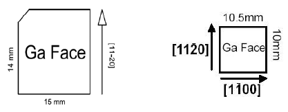
15mm,10mm,5mm GaN Free-standing Substrate
| Item | PAM-FS-GaN50-N | PAM-FS-GaN50-SI |
| Conduction Type | N-type | Semi-insulating |
| Size | 14.0mm*15mm 10.0mm*10.5mm 5.0*5.5mm | |
| Thickness | 230+/-20um, 280+/-20um | |
| Orientation | C-axis(0001)+/-0.5° | |
| Primary Flat Location | ||
| Primary Flat Length | ||
| Secondary Flat Location | ||
| Secondary Flat Length | ||
| Resistivity(300K) | <0.5Ω·cm | >10^6Ω·cm |
| Dislocation Density | <5×10^6cm-2 | |
| Marco Defect Density | 0cm-2 | |
| TTV | <=15um | |
| BOW | <=20um | |
| Surface Finish | Front Surface:Ra<0.2nm.Epi-ready polished Back Surface:1.Fine ground 2.Rough grinded ≥ 90 % |
|
Usable Area
Note:
Validation Wafer:Considering convenience of usage, PAM-XIAMEN offer 2″ Sapphire Validation wafer for below 2″ size Freestanding GaN
For more information, please visit our website: https://www.powerwaywafer.com,
send us email at sales@powerwaywafer.com and powerwaymaterial@gmail.com
Found in 1990, Xiamen Powerway Advanced Material Co., Ltd (PAM-XIAMEN) is a leading manufacturer of semiconductor material in China. PAM-XIAMEN develops advanced crystal growth and epitaxy technologies, manufacturing processes, engineered substrates and semiconductor devices. PAM-XIAMEN’s technologies enable higher performance and lower cost manufacturing of semiconductor wafer.
Our goal is to meet all of your requirements, no matter how small orders and how difficult questions they may be,
to maintain sustained and profitable growth for every customer through our qualified products and satisfying service.