GaAsSb / InGaAs / InP heterostructure is provided by epi-structure MBE grower PAM-XIAMEN for optical sensor fabrication. The gallium arsenide antimonide (GaAsSb) lattice constant is completely matched with the lattice constant of InP substrate, so it is easy for epitaxial growth on InP substrate with good uniformity. The response wavelength of the type-II InGaAs / GaAsSb superlattice detector can be adjusted by changing the layer thickness and structure of each material in the superlattice. GaAsSb / InGaAs superlattices are the preferred material system for a new type of short-wave infrared detectors. Here is listed the spec from PAM-XIAMEN:
1. Specification of GaAsSb / InGaAs Superlattices on InP Substrate
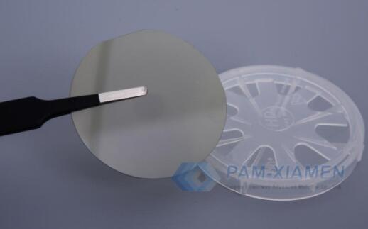
PAM161124 – SLS
| Layer | Composition | Thickness | periods | Carrier Concentration | Dopant |
| Cap Layer | InGaAs or InAlAs | – | 1 | – | Be-doped |
| P Layer | SL-GaAsSb/InGaAs | – | – | – | Be-doped |
| i-Active | SL-GaAsSb/InGaAs | – | – | – | – |
| n Layer | SL-GaAsSb/InGaAs | – | 50 | – | Si-doped |
| Buffer | InGaAs | 50nm | – | – | Si-doped |
| Bottom | InGaAs or InAlAs | – | – | n=1E18 | Si-doped |
| Substrate | InP(100) | 350um | – | – | Si-doped |
2. Fabrication of GaAsSb / InP Epitaxial Wafer
The unintended InGaAs is n-type, the background concentration of i-InGaAs for MBE technology is much lower than MOCVD. Our technology can reach to 7-9E14cm3. If you need lower carrier concentration, we will compensate i-InGaAs by doping Be.
The unintended GaAsSb is p-type, the background concentration of i-InGaAs for MBE technology is nearly 1-5E15cm3, which is much lower than that of MOCVD. And it is easy to achieve lower background concentration by doping Si.
The i-InGaAs layer can be slight p-type, which concentration is 1-5E15cm3 by doping Be. Normally, for InP-based microwave device, we only grow 200nm InAlAs for buffer layer, and it’s enough to eliminate dislocation, defect, stain and surface roughness etc. So we believe 500nm InGaAs is enough for buffer layer, and we will provide EPD<500 InP substrate for you. Your EPI-wafer thickness is more than 4.5um, especially ternary alloy. It needs outstanding skills for growing it.
As for ohmic contact to the above spec, the ohmic contact of p-type InGaAs is better than p-type InAlAs. And Ti/Pt/Au metal is the best for metallization. In addition, the ohmic contact of n-type InGaAs is better than n-type InAlAs. AuGeNi/Au metal is the best for metallization, just like n-GaAs ohmic contact. For good ohmic contact to p-type InGaAs, the mesa etch has to stop more or less in the middle of the layer. As thicker the InGaAs layer as ease it could be done.
3. Effects of Be Doping on the Properties of InGaAs / GaAsSb Epilayers
There is a direct relationship between the carrier concentration in the absorption region of photovoltaic detectors and the performance of the detector. The carrier concentration in the absorption region determines the lifetime and diffusion length of minority carriers, thus affecting the quantum efficiency and the detection rate of the detector. In the InGaAs / GaAsSb II type superlattice detector, the superlattice is used as the absorption region, and the background carriers in the intrinsic superlattice are n-type conductive, which means that the minority carriers of the detector are holes, and the diffusion of holes. The length is smaller than the diffusion length of electrons. If the minority carriers in the absorption region are electrons, the diffusion length of the minority carriers can be increased. Therefore, we used p-type Be to compensate the superlattice material, and studied the relationship between different Be doping temperatures and the properties of InGaAs / GaAsSb quantum well. We found that doping concentration of the superlattice is sensitive to the Be temperature.

For more information, please contact us email at victorchan@powerwaywafer.com and powerwaymaterial@gmail.com.