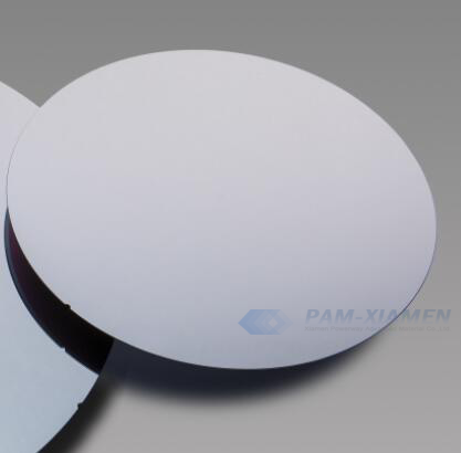
InGaAs quantum well (QW), as a commonly used two-dimensional material in near-infrared band, has important applications in semiconductor lasers, solar cells and other devices. In the field of semiconductor lasers, InGaAs/GaAs quantum well expands the luminous wavelength of GaAs (0.85~1.1 μm) and is widely used in various optoelectronic devices and industrial production activities. PAM-XIAMEN can offer laser wafers in various wavelength, please visit https://www.powerwaywafer.com/gaas-wafers/epi-wafer-for-laser-diode for more wafer information. Therein, the InGaAs quantum-well heterostructure for 1.06um lasers from us is as follows.

1. InGaAs / GaAs Quantum Well Structure for 1060nm High Power Laser Fabrication
No. 1 InGaAs Quantum Well Wafer for High Power Laser
|
InGaAs Quantum Well Wafer for 1.06um High Power Laser (PAM190430-1060LD) |
|||||
| Layer No. | Layer Name | Material | Thickness | Carrier Concentration | Dopant |
| 1 | P-Contact | GaAs | – | – | p-C Doped |
| 2 | Cladding | Al(0.36)Ga(0.64)As | 800 | – | p-C Doped |
| 2 | Cladding | Al(0.36)Ga(0.64)As | – | – | p-C Doped |
| 3 | Graded | Al(0.26-0.36)Ga(0.74-0.64)As | – | 5×10^17 | I |
| 4 | Waveguide Core | Al(0.26)Ga(0.74)As | – | I | |
| 5 | Barrier | GaAsP (Tensile Barrier) | – | I | |
| 6 | Quantum Well | InGaAs (Compressive well) | – | I | |
| 7 | Barrier | GaAsP (Tensile Barrier) | 10 | I | |
| 8 | Waveguide Core | Al(0.26)Ga(0.74)As | – | 1×10^17 | N Si Doped |
| 9 | Graded | Al(0.26-0.32)Ga(0.74-0.64)As | – | – | N Si Doped |
| 10 | Cladding | Al(0.32)Ga(0.68)As | – | – | N Si Doped |
| 11 | Buffer | GaAs | 250 | – | N Si Doped |
| 12 | Substrate | N-doped GaAs Substrate | |||
No.2 LD Structure Grown with GaInAs QW
PAM220829 – 1060LD (universal)
| Layer No. | Material | Thickness | Doping Concentration |
| 6 | P+ GaAs | – | (0.5~2) x 1020cm-3 |
| 5 | P- GaAs | 1.2um | – |
| 4 | AlGaAs | – | – |
| 3 | GaInAs QW, PL: 1030-1060nm | – | – |
| 2 | AlGaAs | 0.6um | – |
| 1 | N- AlGaAs | – | – |
| 0 | N GaAs (100) substrate, 2° or 15° off towards <111>A | 350~450um | (0.4~4) x 1018cm-3 |
2. Role of GaAsP Barrier in InGaAs Quantum Well Growth
The maser wavelength of semiconductor laser is mainly determined by material components, quantum well width, strain variables and other factors. The InGaAs/ InGaAsP material system is used to grow the laser wafer. In order to extend the maser wavelength of InGaAs strain quantum well beyond 1um, the In component must be increased.
However, in the wavelength range of 1000-1100 nm, there will be a large lattice mismatch between InGaAs quantum wells with higher In content and GaAs. When the lattice mismatch is close to 2%, defects such as dislocations are prone to occur. This will not only affect the epitaxial crystal quality, but also affect the performance, life and reliability of the InGaAs QW lasers. Therefore, for high-strain quantum well materials, the introduction of strain compensation structure can solve the problem of strain accumulation and improve the epitaxial crystal quality.
GaAsP is a typical tensile strain material. The lattice constant of GaAsP ranges from 5.45 to 5.65, which is smaller than GaAs. At the same time, its energy band width ranges from 1.42 to 2.77, this is much larger than that of GaAs and InGaAs. So GaAsP is very suitable to be used as the barrier of InGaAs quantum well. Form strain compensation structure.
The results show that a GaAsP tension barrier layer outside InGaAs quantum well can enhance carrier limiting ability of 0.98um and 1.06um quantum wells. GaAsP tension barrier can improve the ability of InGaAs QW to capture carriers, thereby reducing the threshold current density and improving the internal quantum efficiency. And the InGaAs quantum well laser diodes using GaAsP barrier layer have higher power and better temperature stability at high temperature.
Remark:
The Chinese government has announced new limits on the exportation of Gallium materials (such as GaAs, GaN, Ga2O3, GaP, InGaAs, and GaSb) and Germanium materials used to make semiconductor chips. Starting from August 1, 2023, exporting these materials is only allowed if we obtains a license from the Chinese Ministry of Commerce. Hope for your understanding and cooperation!
For more information, please contact us email at victorchan@powerwaywafer.com and powerwaymaterial@gmail.com.

