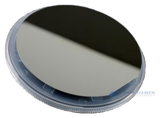
Ternary compound semiconductor material InxGa1-xAs is a mixed solid solution formed by GaAs and InAs. It is a sphalerite structure and belongs to direct bandgap semiconductor. Its energy band changes with the change of alloy and can be used to make various photoelectric devices, such as HBT, HEMTs, FET, etc. The band gap width of InxGa1-xAs is from 0.35eV(3.5μm) of InAs to 1.42eV(0.87μm) of GaAs. Therein, the gap width of In0.53Ga0.47As matched with InP substrate lattice is 0.74eV(1.7μm), which has been widely used in 0.9 ~ 1.7μm band, such as optical fiber communication, night vision and so on. We are able to provide epitaxial wafers for fabrication of InGaAs photodiode. The detailed InGaAs / InP photodiode epi structures are as follows:
1. InP / InGaAs Photodiode Stack Structure
At present, devices based on InGaAs photodiode array mainly have two different structures: mesa type and planar type. We can grow both types of epitaxial structures below for InGaAs photodiode chip fabrication.
1.1 Epitaxy Structure for Making Mesa InGaAs PIN Photodiode
|
Mesa Device Stack of InGaAs / InP (PAM190304-INGAAS) |
|
| Epi Layer | Thickness |
| p-InGaAs | – |
| i-InGaAs | – |
| n-InP buffer layer | 0.3-0.7um |
| InP substrate | |
1.2 Epitaxy Structure for Making Planar InGaAs Photodiode
|
InGaAs Planar Device Stack (PAM190304-INGAAS) |
|
| Epi Layer | Thickness |
| i-InGaAs contact layer | – |
| n-InP cap layer | 0.9-1um |
| n-InGaAs interface layer (optional) | – |
| i-InGaAs | – |
| n-InP buffer layer | – |
| n type InP substrate | |
2. What Are Mesa Structure and Planar Structure of InGaAs Photodiode Wafer?
Mesa type transistors (diodes and triodes) are relative to planar transistors, and the structure appears as a Mesa shape, so it is the so-called mesa structure. Mesa structure can eliminate the bending part of the P-N junction in the planar structure, so that the P-N junction is perpendicular to the side surface of the semiconductor wafer. The surface electric field of the P-N junction is relatively low, which can ensure that the breakdown of the P-N junction is basically the avalanche breakdown in the body, avoiding the lower surface breakdown, so as to improve the voltage resistance performance of the device.
The mesa structure is usually obtained by grinding or polishing, but in today’s InGaAs phodiode chip manufacturing process can often be achieved by grooving or etching on the P+-i-N+ structure doped in situ.
However, planar device is based on N-i-N+ structure of InGaAs / InP by ion implantation or diffusion method to form PN junction. The advantage of this method is that PN is buried in the material, isolated from the outside so that the dark current and noise is relatively small.
Remark:
The Chinese government has announced new limits on the exportation of Gallium materials (such as GaAs, GaN, Ga2O3, GaP, InGaAs, and GaSb) and Germanium materials used to make semiconductor chips. Starting from August 1, 2023, exporting these materials is only allowed if we obtains a license from the Chinese Ministry of Commerce. Hope for your understanding and cooperation!

For more information, please contact us email at victorchan@powerwaywafer.com and powerwaymaterial@gmail.com.