Silicon carbide (SiC) is a hot research material in the field of quantum information technology. For example, defect vacancies in SiC (composed of silicon vacancies and adjacent carbon vacancies, hereinafter referred to as VV) have many advantages of NV centers in diamond, including triple ground states and the advantage of mature main material research technology. The location of material defects can, in principle, be located on specific surfaces or interfaces, and the presence of defects is particularly important for sensing applications. In terms of integration with other systems, the connection between spin defects and photonic cavities has been proposed as an effective means of interaction between photons and optically addressable spin defects, which is a key feature of quantum communication applications. For example, cubic polytype silicon carbide (3C SiC) has been used to construct photonic cavities with high quality factors and achieve the incorporation of VV defects in the material. The prerequisite for achieving effective integration of nanostructures and materials is to study and understand spin defects near the surface and interface.
PAM-XIAMEN can supply N type 3C-SiC substrate, specifications as listed in: https://www.powerwaywafer.com/3c-sic-wafer.html.
Researchers used first principles calculations to investigate the physical properties of near surface defect vacancies in 3C SiC, and considered rich silicon (001) surfaces with various reconstructions and terminations. Near the surface of SiC (2×1): H, VV is a stable and elastic spin defect with little variation in characteristics compared to bulk defects. In addition, the research results on the functional relationship between spin defects (VSiVC) and surface reconstruction and termination of – H, – OH, – F, and oxygen groups in 3C SiC indicate that 3C SiC is a promising quantum application material.
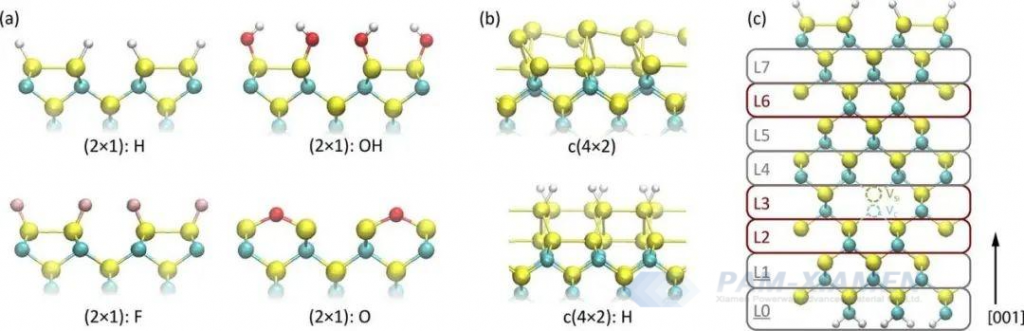
Fig. 1 Atomic structure of the 3C SiC (001) surface rich in silicon. (2×1):H model As shown in the side view, the electronic structure of the defect is studied as a function of its proximity to the surface: L2 is the position closest to the fixed layer, L3 is in the middle of the model, and L6 is the position closest to the surface.

Fig. 2 Calculating the electronic structure of the neutral double vacancy at L3 in the surface silicon rich 3C SiC (001) plane using PBE and HSE functionals. The results indicate that at the PBE and HSE theoretical levels, all functional trends of surface terminals are the same. Therefore, the saturation of hydrogen atoms on the reconstructed (2×1) surface will lead to the most promising surface structure.

Fig. 3 Energy difference (eV) between bulk 3C-SiC VV and near surface VV under PBE functional

Fig. 4 Calculation of surface electron affinity (EA) of (2×1) (001) rich silicon carbide (2×1) rich silicon surface
Considering the symmetry breaking introduced by the surface, it is crucial to understand its impact on the zero field splitting (ZFS) tensor component values. In Table 2, this article reports the calculated ZFS components of VV for four different surface terminals located in the middle of the (2×1) model (L3). The E component of zero field splitting has a significant sensitivity to the position of defects relative to the surface, indicating that this parameter can be used as an indicator of defect proximity to the surface. Finally, qualitative studies on volume and surface Debye Waller factor (DWF) indicate that the decrease in surface DWF can be alleviated through strain engineering of SiC samples.

Fig. 5 Calculation components D and E of zero field splitting (ZFS) tensors for 3C SiC bulk and near surface neutral VV ground states with different surface terminations

For more information, please contact us email at victorchan@powerwaywafer.com and powerwaymaterial@gmail.com.