Silicon wafer bonding technology refers to the method of tightly combining silicon wafers with silicon wafers, silicon wafers with glass or other materials through chemical and physical interactions. Silicon wafer bonding is often combined with surface silicon processing and bulk silicon processing, and is used in MEMS machining processes. PAM-XIAMEN can supply silicon wafer for wafer bonding applications with following specification for example:
1. Silicon Wafer Specification
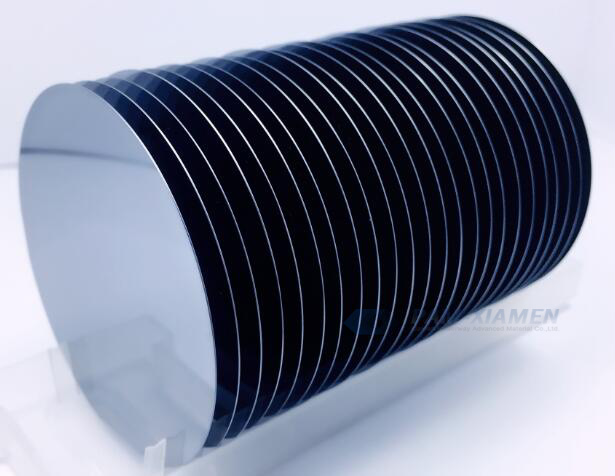
PAM210721 – SI
Silicon wafers, per SEMI Prime, P/E 6″ (150.0±0.2mm)Ø×625±15µm,
p-type Si:B[100]±0.5°, Ro=(1-100)Ohmcm,
One-side-polished, back-side etched,
2 SEMI Flats:
Primary Flat: 57.5±2.5mm @ 111±1°,
Secondary: 37.5±2.5 mm@ 90±5° CW from PF,
Particles <20@0.2µm,
Sealed in Empak or equivalent cassette,
CtQ: Particles <20@0.2µm,
TTV <10, Bow <30, Warp <30
2. Silicon Wafer Bonding Techniques
Common silicon wafer bonding technologies include gold silicon eutectic bonding, silicon/glass electrostatic bonding, silicon/silicon direct bonding, glass solder sintering and etc. Here we just briefly introduce the first three techniques as follows:
2.1 Gold Silicon Eutectic Bonding
Gold silicon eutectic bonding is often used in the packaging of microelectronic devices. The Si-Si wafer bonding process in gold-silicon eutectic involves thermal oxidation of p-type (100) crystalline silicon wafers, followed by evaporation of a 30nm thick titanium film onto the wafers using electron beam evaporation, followed by evaporation of a 120nm gold film. This is because the titanium film has a higher adhesion to the SiO2 layer. Finally, place the two silicon wafers together on the heater, add a mass block to compact, and anneal at a temperature of 350-400℃. The experiment shows that at an annealing temperature of 365℃ and a time of 10 minutes, the bonding surface exceeds 90%. The time and silicon wafer bonding temperature are crucial.
In addition to gold, Al, Ti, PtSi, and TiSi2 can also serve as intermediate transition layers for silicon – silicon bonding.
2.2 Electrostatic Bonding
Electrostatic bonding, also known as field assisted bonding or anodic bonding. Electrostatic bonding technology can bond glass with metals, alloys, or semiconductors without any adhesive. This type of bonding has low temperature, firm bonding interface, and good long-term stability.
There are many factors that affect electrostatic bonding, mainly including:
1) The thermal expansion coefficients of two electrostatic bonding materials should be approximately matched, otherwise they will break due to high internal stress during the cooling process after bonding;
2) The anode shape affects the bonding effect. The contact electrodes and parallel plate electrodes are commonly used. Point contact electrode, bonding interface will not generate pores, while double parallel plate electrode, bonding interface will have some pores, and bonding rate will be faster;
3) The wafer surface condition also affects the bonding force. The higher flatness and cleanliness of the bonding surface will obtain a better bonding quality. A greater surface undulation will make electrostatic attraction smaller. The same fluctuation amplitude on the surface, the smoother the fluctuation, the greater the electrostatic attraction.
2.3 Direct Silicon Wafer Bonding
Two silicon wafers can be directly bonded together through high-temperature treatment, without the need for any adhesive or external electric field, and the process is simple. This bonding technology is called silicon direct bonding (SDB ).
The silicon direct wafer bonding process is as follows:
1) Soak two polished silicon wafers (both oxidized and unoxidized) in a solution first;
2) Affix two silicon wafers at polished sides together at room temperature;
3) The bonded silicon wafer undergoes several hours of high-temperature treatment in an oxygen or nitrogen environment, forming good silicon bonding.

For more information, please contact us email at victorchan@powerwaywafer.com and powerwaymaterial@gmail.com.