Silicon wafers can be supplied with specifications as found in: https://www.powerwaywafer.com/silicon-wafer
Silicon is a semiconductor material, and its resistivity is closely related to the doping concentration. Doping is that introducing a small amount of impurities into silicon crystals to alter their electrical properties. According to the requirements of conductivity type and resistivity, V-group elements (such as P, As, Sb, Bi) should be selected to prepare N-type silicon single crystals; while the preparation of P-type silicon requires Group III elements (such as B, Al, Ga, In, Ti). The content of impurity elements in silicon crystals determines the electrical resistivity of silicon single crystals.
1. The Relationship Between Resistivity and Impurity Concentration
The resistivity is not only related to impurity concentration, but also to the mobility of charge carriers. When the concentration of impurities is high, impurities have a scattering effect on charge carriers. It can greatly reduce the mobility of charge carriers, thereby affecting the conductivity of silicon crystal. Thus, the relationship curve between resistivity and impurity concentration was theoretically calculated as shown in Fig. 1.
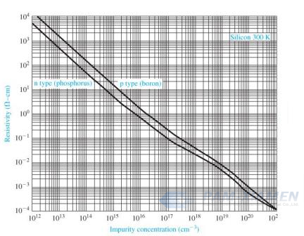
Fig. 1 Relationship between resistivity and impurity concentration of silicon
The resistivity is influenced by both carrier concentration (impurity concentration) and mobility, so the resistivity and impurity concentration are not linearly related.
For non intrinsic semiconductors, the electrical resistivity of a material is mainly related to the majority carrier concentration and mobility.
When the impurity concentration increases, the curve deviates significantly from the straight line, mainly due to:
1) Impurities cannot be completely ionized at room temperature;
2) The mobility significantly decreases with the increase of impurity concentration.
Due to the different mobility of electrons and holes, the intrinsic conductivity of a semiconductor may not necessarily be the smallest at a certain temperature.
2. The Relationship Between Resistivity and Temperature
In the moderate temperature range dominated by non intrinsic excitation (approximately between 200K and 450K), impurities are completely ionized, and the concentration of electrons remains basically unchanged. However, due to the decrease in carrier mobility with increasing temperature within this temperature range, the conductivity of semiconductor materials also shows a slight decrease with increasing temperature. When the temperature further increases, it enters the intrinsic excitation region, and the concentration of intrinsic charge carriers increases rapidly with the increase of temperature, so the conductivity also increases rapidly with the increase of temperature.
When the temperature is relatively low, due to the freezing effect of impurity atoms, the carrier concentration and the conductivity of the semiconductor material continuously decrease with the decrease of temperature.
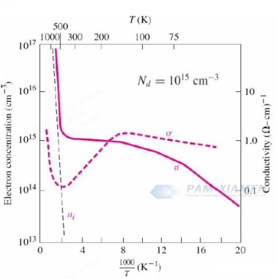
Fig. 2 Electron concentration and conductivity versus inverse temperature for silicon
As shown in Fig. 2, when the doping concentration N of donor impurities is 1E15cm-3, the relationship curve between the electron concentration and its conductivity in silicon with temperature changes.
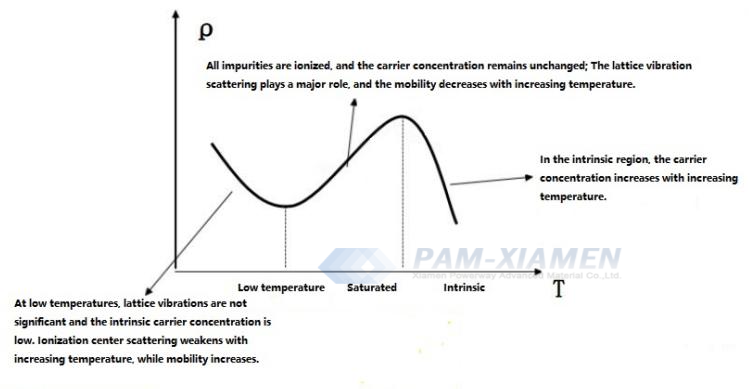
Fig. 3 Relationship between resistivity and temperature changes
There are three types of doping in the production process based on the high and low electrical resistivity:
Light doping, suitable for single crystals applied in high-power rectifier;
Medium doping, suitable for single crystals used in transistor;
Heavy doping, ideal for single crystal substrate for epitaxial growth.
Considering the thermal stability of the entire semiconductor device and in the manufacturing process of semiconductor devices, especially in high-temperature processes such as diffusion and epitaxy, it is often required that the diffusion coefficient of doped elements in silicon single crystals be smaller and better. Otherwise, when high-temperature diffusion is used to make devices, impurities on the substrate also enter the epitaxial layer through anti diffusion, affecting the redistribution of impurities and adversely affecting the electrical performance of the device.

For more information, please contact us email at victorchan@powerwaywafer.com and powerwaymaterial@gmail.com.