PAM-XIAMEN can supply AlN single crystal substrate, additional specification please refer to https://www.powerwaywafer.com/aln-substrate.html.
The main n-type AlN candidate dopants are oxygen (O) and silicon (Si), while for p-type AlN, they are magnesium (Mg) and beryllium (Be). So far, the success rate of Mg and O doping has been very low. However, O is an important compensating impurity for both Mg and Be, as both dopants and Al itself tend to absorb oxygen. To understand the doping of AlN, it is necessary to understand the roles of nitrogen vacancies (VN) and aluminum vacancies (VAl) and their related complexes. The current understanding of defect and impurity chemistry, as well as non-equilibrium doping methods, will be considered a promising approach to overcome current technological limitations.
1. Donor Doping of AlN: Silicon
For n-type AlN, silicon is the optimal theoretical cation donor because its atomic radius is very close to that of Al, as shown in Fig. 1 (Al is 118 pm, Si is 111 pm). Although silicon is a shallow donor in GaN with an activation energy ED of approximately 17 meV, in AlGaN, with an increase in Al content, its ED increases from 24 meV in Al0.85Ga0.15N to 211 meV in Al0.96Ga0.04N. Silicon, as a substitute impurity in AlN, causes a theoretical contraction of 6% in the nearest neighboring basal plane N bond. This indicates a decrease in the position of the silicon lattice, closer to the three basal bonds, during which the Si-N c-axis bonds are stretched. When silicon captures a secondary electron and undergoes geometric rearrangement, a DX center is formed, which includes a 2% contraction of Si-N bonds at three basal positions and a c-axis Si-N bond rupture, as shown in Fig. 1, leading to a transition from shallow to deep level states. When the c-axis Si-N bond under stress breaks, a compensated deep state will be generated. Despite the existence of such compensation defects, n-type doping of AlN through ion implantation in the near surface region has shown promising results. However, in the n-type doping of uncompensated MOCVD AlN thin films, only a reproducible electron concentration of up to 1015 cm-3 is displayed, which is only applicable to high drift field regions in the device.
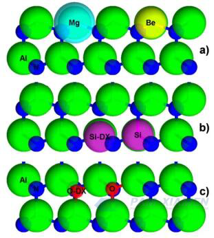
Fig. 1 The positions and relative sizes (in proportion) of (a) Mg and Be acceptors in AlN, (b) Si impurities rearranged by Si donors and DX, and (c) positions and relative sizes of oxygen defects substituted for oxygen and DX rearrangements (in proportion)
Given that one technology demonstrates the feasibility of doping while another technology does not, silicon itself cannot be the problem. The hypothesis that non-equilibrium and low-temperature MBE contribute to n-type doping of AlN is based on the following two points:
1) when using low temperature, the minimum thermal expansion is achieved, therefore the minimum additional c-axis Si-N bond elongation is desirable;
2) Minimizing metal enrichment conditions for Al vacancy Si complexes, these complexes exhibit behavior similar to Al vacancy O complexes, leading to self compensation of donor doping at high Si doping levels.
It is speculated that this Si self compensation is due to lattice softening caused by VAl, which makes it easier to break the c-axis Si-N bond and thus form a compensated Si-DX center. Similar to O, due to charge neutrality, the VAl-XSiAl complex must also be considered, where X is an integer. Therefore, claiming non-equilibrium, low-temperature, and metal enriched MBE is very valuable for n-type doping of AlN.
2. Acceptor Doping of AlN: Mg, Be, and C
For p-type AlN, acceptors, like anion substituted carbon (C) and cation substituted Be and Mg are considered feasible. When approaching the dilution limit, isolated acceptor energies result in these acceptors being considered as deep level receptors, with theoretically reported single valued acceptor activation energies for Mg and Be ranging from 510 to 630 meV and 220 to 340 meV, respectively. If there is no ability to form impurity bands to reduce these large activation energies, significant pore concentration is not expected.
However, as shown by the Bohr orbital overlap at high doping concentrations in GaN, it is possible for the effective activation energy of Mg to decrease from about 210 meV to about 50 meV, resulting in a pore concentration of 1 x 1020 cm-3. This has also been proven to be effective for AlGaN with up to about 60% Al, and tunnel diodes have been demonstrated.
Apart from a pore concentration of approximately 1010 cm-3, Mg has not been successfully used for doping AlN. The recent results of using Be to obtain a room temperature pore concentration of approximately 3 x 1018 cm-3 (reported here as approximately 4.4 x 1018 cm-3) and an effective activation energy of approximately 37 meV indicate that a reduction in activation energy can be achieved.
The relative dielectric constants of gallium nitride (GaN), aluminum nitride (AlN), and indium nitride (InN) are 8.9, 8.5, and 15.3, respectively. The reported effective masses of heavy holes are 0.8mo, 3.53mo, and 1.63mo, respectively. This means that the Mott critical concentrations formed by the acceptor bands of GaN, AlN, and InN are approximately 4×1019cm-3, 4×1021cm-3, and 6.5×1019 cm-3, respectively. This simplified approximation is in good agreement with the doping results of metal modulated epitaxy (MME) experiments for GaN, where hole concentrations in the range of 1019 cm-3 can be routinely achieved. Similarly, these predictions indicate that AlN and InN will be more difficult to undergo degenerate p-type doping, each requiring a higher doping concentration to form impurity bands.
For AlN, it may initially be considered impossible to achieve the high doping concentration required to form impurity bands, which is contrary to current experimental results. However, it is necessary to consider the unique valence band structure of AlN, where the split off band is actually higher than the hole band and light hole band (see Fig. 2), and has high anisotropy. Due to the lack of d-orbital electrons, the sign of crystal field splitting energy is opposite to that of GaN. The splitting off band exhibits greater curvature and is located on a wider range of heavy and light hole bands in terms of energy. Fig. 2 shows the density functional theory (DFT) calculation considering this effect. The effective masses calculated by density functional theory (DFT) are 3.66mo for the parallel component and 0.24mo for the vertical component, resulting in Mott critical concentrations of 4.3×1021 cm-3 and 1.2×1018 cm-3, respectively. The upper and lower limits of the Mott critical concentration are given to emphasize that when considering the uniqueness of the AlN band structure, it is possible to predict the formation of impurity bands in AlN, which may lead to higher hole mobility than GaN, bringing hope for p-channel and bipolar AlN devices.
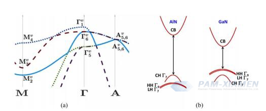
Fig. 2 (a) Density functional electron dispersion of the linear trajectory of the unstressed AlN valence band (spin free) of wurtzite along the M, Γ and A symmetry points within the Brillouin zone. At the center of the region, split off band states ΓV1 is singlet degeneracy, while heavy and light hole states ΓV 6 is doubly degenerate. (b) Qualitative electron dispersion of unstressed wurtzite AlN and GaN along the k⊥ direction. Unlike GaN, the highest valence band in AlN is the dissociation band, which exhibits a smaller effective mass. The introduction of spin orbit interaction relieves the degeneracy of heavy and light hole bands in the region center, resulting in the emergence of a single degenerate state ΓV; 17, ΓV9 and Γ V;27.

For more information, please contact us email at victorchan@powerwaywafer.com and powerwaymaterial@gmail.com.