High quality polycrystalline CdZnTe films were prepared by aluminum induced crystallization (AIC) and radio frequency (r.f.) magnetron sputtering. The crystallinity, morphology and optical property of both as-deposited and AIC samples were investigated by X-ray diffraction (XRD), and atomic force microscopy (AFM), as well as Raman and ultraviolet–visible spectrometry. The results of XRD showed that AIC favours the preferential orientation [1 1 1], and promotes the crystallinity of the CdZnTe films. AFM micrographs show that the grain size was increased from 50 nm to 300 nm after AIC. In the Raman spectrum of CdZnTe films, the intensity of CdTe-like TO mode is enhanced after AIC. From the optical transmittance and absorption coefficient, the value of the band gap varied from 1.53 eV to 1.65 eV.
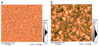
Fig. 1. AFM micrographs (15 μm×15 μm) for the CdZnTe films: (a) as-deposited and (b) Al-induced.
Source: sciencedirect
If you need more information about Effect of Al-induced crystallization on CdZnTe thin films deposited by radio frequency magnetron sputtering, please visit our website:https://www.powerwaywafer.com/, send us email at sales@powerwaywafer.com or powerwaymaterial@gmail.com.