Experimental and theoretical investigation of phosphorus in-situ doping of germanium epitaxial layers
We investigate phosphorus in-situ doping characteristics in germanium (Ge) during epitaxial growth by spreading resistance profiling analysis. In addition, we present an accurate model for the kinetics of the diffusion in the in-situ process, modeling combined growth and diffusion events. The activation energy and pre-exponential factor for phosphorus (P) diffusion are determined to be 1.91 eV and 3.75 × 10⁻⁵ cm2/s. These results show that P in-situ doping diffusivity is low enough to form shallow junctions for high performance Ge devices.
Highlights
► We investigate the phosphorus in-situ doping characteristics in germanium.
► Phosphorus in-situ doped profile exhibits a box-shaped junction formation.
► The modeling and the experimental results are in very good agreement.
► Phosphorus in-situ doping diffusivity is low enough to form shallow junction.
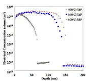
Fig. 1. SRP depth profiles of P in 400 °C, 500 °C, and 600 °C in-situ doped Ge layer growth for 2 min.
Source: Current Applied Physics
If you need more information about Experimental and theoretical investigation of phosphorus in-situ doping of germanium epitaxial layers, please visit our website:https://www.powerwaywafer.com/, send us email at sales@powerwaywafer.com or powerwaymaterial@gmail.com