What we provide:
Item
undoped N-
Si doped N+
Semi-insulating
P+
Freestanding GaN substrate
yes
yes
yes
GaN on sapphire
yes
yes
yes
yes
InGaN on sapphire
yes
***
AlN on sapphire
yes
LED wafer
(p+GaN/MOW/N+GaN/N-AlGaN/N+GaN/N-GaN/sapphire)
Freestanding GaN substrate/GaN on sapphire/LED wafer:
For specifications of Freestanding GaN substrate/GaN on sapphire/LED wafer, please view Gallium Nitride wafer:
http://www.qualitymaterial.net/products_7.html
InGaN on Sapphire:
For specification of InGaN on sapphire template, pleas view InGaN substrate:
https://www.powerwaywafer.com/InGaN-Substrates.html
AlN on [...]
2019-09-24meta-author
Undoped InP Wafer
PAM-XIAMEN offer low doped InP wafer substrate, see the following:
InP wafer,2” (PAM-190507-INP)
Diameter – 50.8±0.5 mm;
Thickness – 350±25 µm;
N type, low doped
Dopant – low doped
Orientation – (100)±0.5°
Flat orientation – SEMI-E/J;
Major flat orientation – (0-1-1) ±0.5°
Major flat length – 16.0±1.0 mm;
[...]
2020-03-18meta-author
PAM XIAMEN offers Coated Silicon wafer.
Nickel <111> Film( 100nm) Coated Si Wafer (100) P/Boron ,10x10x0.5mmSSP, R:1-20 ohm.cm
Nickel <111> Film( 100nm) Coated Si Wafer (100) P/Boron ,5x5x0.5mmSSP, R:1-20 ohm.cm
Nickel<111> Film (100nm) Coated SiO2/Si Wafer -(100) P/Boron ,10x10x0.5mmSSP, R:1-20 ohm.cm
Nickel<111> Film (100nm) [...]
2019-04-28meta-author
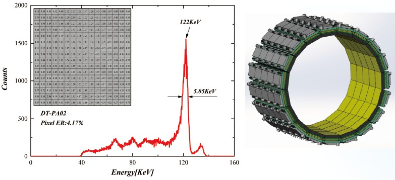
PAM-PA03 series are pixel electrode structured detectors based on CZT crystal.
1. CZT Compton Imaging Detector Specification
Material
CdZnTe
Density
5.8g/cm3
Volume resistivity
>1010Ω.cm
Dimension
22.0×22.0 mm2
Thickness
15.0mm
Pixel size
1.38×1.38 mm2
Pixel center space
1.88mm
Pixel array
11×11
Electrode material
Au
Operation temperature
25℃-+40℃
Energy range
60KeV~2.6MeV
Energy resolution(22℃)
Average pixel <5%@662KeV
Storage temperture
10℃~40℃
Storage humidity
20%-80%
2. Spectrum of CZT Compton Imager
3. Features Compton Imaging Detector Based on CZT Crystal
Long-time stability
High energy [...]
2019-04-24meta-author
Single crystal germanium wafer with orientation (110) miscut toward <111> with 4 deg. or 12 deg. is provided without dopant. Due to the similar chemical properties with silicon, single crystal germanium has similar applications. While hall effect germanium wafer has higher sensitivity to gamma [...]
2021-10-25meta-author
New research of SiC and GaN technology along with LED technology can be shared, and we can send you paper content if you want. Please see below article title:
No.1 Technologies for Power Electronics and Packaging (SiC & GaN)
1-1.The latest development of SiC power devices
1-2.New Progress of SiC high voltage power electronic devices and applications
1-3.SiC MOSFET Device Structure and Process Study
1-4.Electro-thermal Analysis of 1.2kV-100A SiC JBS Diodes Under Current Overload
1-5.Graphene-on-SiC for gas detection and bio-sensors
1-6.Packaging of high-voltage wide-bandgap power semiconductors
1-7.High power & high temperature IGBT and WIDE bandgap power semiconductor modual package
1-8.Design and TCAD Simulation of Widegap Semiconductor Devices
1-9.GaN Power Devices Beyond 650V and 150C
1-10.High-breakdown voltage GaN HEMTs fabricated on semi-insulating GaN substrates
1-11.A Gate Driver IC for E-mode GaN HEMTs with Reverse Conduction Detection
1-12.Development of Normally-off AlGaN/GaN HFETs for Power Electronics
1-13.High crystal quality GaN-on-Si to achieve excellent isolation and dynamic performance without carbon doping
1-14.200mm/8-inch GaN power device and GaN-IC technology: a new opportunity for wafer suppliers, foundries and IDMs
1-15.200mm 40V-650V E-mode GaN-on-Si Power Technology: from Device, Package, Reliability to System
1-16.GaN, Power the Future
1-17.AlGaN/GaN heterostructure pH sensors with high Al composition in the barrier layer
1-18.In-situ Wafer Cleaning for Pre-Epitaxial Deposition for Next Generation Semiconductor Devices
No.2 Micro-LED and other Novel Display
2-1.A New Concept for Fabricating CMOS-driven, High-Performance MicroLED Displays
2-2.Study on three dimensional thermal transport in micro-LEDs at the level of kW/cm2
2-3.1 bin wavelength uniformity on 200 mm GaN-on-Si LED for micro LED application with precise strain-engineering
2-4.Integration of III-V LEDs with Silicon Thin Film Transistors for Micro-LED Displays
2-5.NAURA product solutions for Mini-LED and Micro-LED
2-6.Driving Micro LED to future Lighting and Display
2-7.Growth and fabrication of semi / non-polar LEDs and Micro-LEDs using nano-patterning technology
2-8.Imaging Light Measurement Device for Subpixel evaluation of Micro-LED and OLED Displays
2-9.China LED Display Application Industry Development Report 2018-2019
2-10.Enabling the Next Era of Display Technologies by Micro LED MOCVD Processing
2-11.Research Progress and Prospects of LED Chips for Next Generation Display Application
2-12.Influence of the Charge Transfer on the Lifetime of Quantum-Dot Light-Emitting Diodes
2-13.Low toxic quantum dots polymer nanocomposites for LED applications
2-14.Micro/Mini-LED: From Backlight to Direct-view Display
2-15.Application of COB Integrated Packaging Technology in UHD LED Display Field
2-16.Prospect analysis of the 4-in-1 technical approach in LED Display Field
2-17.Mini LED, Future Directions and Solutions – from Chipone Technology
2-18.Progress in Cooperation Between LCD and LED Industry
No.3 Technologies for Ultra-Wide Bandgap Semiconductor
3-1.An (AlxGa1-x)2O3 metal-semiconductor-metal VUV photodetector
3-2.Growth and Characterization of Ultra-Wide Bandgap Oxide Semiconductors
3-3.Progress of diamond ultra-wide-band-gap semiconductor material and devices
3-4.Application of Polycrystalline Diamond Micro-nano Powder in SiC Wafer Processing and Its Key Process Technology
3-5.Epitaxial Growth of Hexagonal Boron Nitride Films on AlN/Sapphire Templates by MOVPE
3-6.Preparation and photoelectric properties of BN films by RF-sputtering
3-7.High quality h-BN thin films and their application as flexible buffer layer for III-nitrides epitaxy
No.4 The Technology in Substrate, Epitaxy and Wafer Growth Equipment (SiC&GaN)
4-1.Synchrotron x-ray diffraction-based visualization of lattice-plane tilting of a GaN substrate and epitaxial film
4-2.In situ coherent x-ray studies of surface dynamics during OMVPE of GaN
4-3.Modeling of SiC crystal growth and epitaxy and simulation of GaN Metal Organic Vapor Deposition
4-4.The effect of n-p electrodes upon the p-type conductivity of B0.375GaN/B0.45GaN QW/QB edge emitting laser diode grown over sapphire substrate
4-5.INDUSTRY4.0 as A Major Opportunity for Electronics Processes and Products
4-6.Interrelationship Between Equipment and PVT Crystal Growth in Silicon Carbide
4-7.Advanced Chemical Concentration Control for Fabrication of Devices Using SiC
4-8.The step growth mechanism for 4H-SiC with Improved Single Polytypes
4-9.Investigation of Defect Levels of Al/Ti 4H-SiC Schottky Structures by Deep Level Transient Spectroscopy
No.5 LED Chip, Packaging, and Modules
5-1.Possible Futures for LEDs and LED Packaging
5-2.Beyond Illumination | Latest Photonics Technology, Breakthrough and Application Trend
5-3.Violet Chip Excited White LEDs for Sun-Like Lighting and Horticulture Lighting
5-4.Research and application for warm white LED of high-efficiency tri-color rare earth Phosphors by purple light Excitation
5-5.Recent progress of fluorescent materials for high-power LED
5-6.Simultaneously improve the luminous efficiency and color rendering index of GaN-based white light emitting diodes using metal localized surface plasmon resonance
5-7.Thermal Simulations of a UV LED module with nanosilver sintered die attach process on graphene coated copper substrates
5-8.Recent progress on massive transfer and integration technologies of Mini & Micro-LEDs
5-9.Anisotropic Conductive Paste and Grip Ring Direct process for mini LED die attachment
5-10.Monolithic Integrated Device of GaN Micro-LED with Graphene Transparent Electrode and Graphene Driving Transistor
5-11.GaN/Si LEDs: Towards Longer Wavelength and Smaller Current Density
5-12.Recent Advances in Achieving Ultra-High Efficiency InGaN-based LEDs
5-13.The effect of air-cavity structure on the process of vertical GaN-based light emitting diodes
5-14.A Wavelength Stabilized GaN based Laser Utilizing Distributed Bragg Reflector
No.6 RF Technology and 5G Mobile Communication
6-1.The Epi structure and Process Considerations of 6-inch GaN RF HEMT for 5G applications
6-2.High frequeny GaN HEMTs and MMICs
6-3.5G mm Wave
6-4.High-frequency GaN-on-Si transistors
6-5.Development and trend of 5G RF Devices and Circuits
6-6.High-linearity GaN HEMTs for millimeter-wave applications
6-7.A Highly Integrated Multi-Parameters RF Module for Microwave Semiconductor Testing
6-8.A Compact X-band Pallet Power Amplifier Using GaN MMIC and Discrete FETs with HMIC Technology
No.7 [...]
2019-12-02meta-author