As one of the leading GaN on silicon companies, PAM-XIAMEN offers GaN on Silicon wafer Substrate. Single crystal silicon wafer substrate is undoubtedly the most potential substrate material for growing III Nitride template due to the advantages of high quality, low price, easy cleavage and etc. The specifications of GaN on silicon epitaxy are listed as following:
1. Specifications of GaN on Silicon Wafer
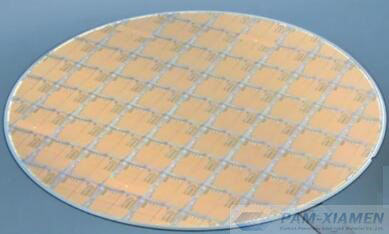
GaN Template ( 100nm) on Silicon Wafer, 10×10 mm;
GaN Template ( 200nm) on Si Wafer, 10×10 mm;
GaN Template ( 500nm) on Silicon Substrate, 5×5 mm;
GaN Template on 2″ Silicon Wafer, GaN film, N type, undoped on Si (111) substrates, 2″x 500 (+/-5%) nm.
2. Development Status and Epitaxial Challenges of GaN on Silicon Technology
GaN-based semiconductor materials have the characteristics of wide direct band gap, high electron saturation drift rate, high breakdown field strength, corrosion resistance, radiation resistance, and good thermal stability. They are the preferred materials for the development of semiconductor optoelectronic devices and high temperature and high power device. However, the application of GaN materials has been limited due to the lack of a suitable substrate.
2.1 GaN on Silicon Wafer Development Status
At present, GaN template on sapphire and GaN on silicon carbide substrate grown by the MOCVD method are relatively mature. However, sapphire is not an ideal substrate material. Its high hardness and difficult-to-dissociate properties makes substrate polishing and device manufacturing difficult. Its poor thermal conductivity is not conducive to the heat dissipation of power chips, and the insulation further restricts the manufacture of planar devices only. In addition, the cost of SiC substrate is very high, which is much higher than that of Si wafer, and it is not suitable for preparing large-area GaN thin film. Furthermore, the processing of SiC devices is also very complicated, both of which are unacceptable for industrialization.
Si substrate has the advantages of good electrical conductivity, thermal conductivity, high crystal quality low cost and easy integration of silicon-based devices. Therefore, although there is a huge mismatch between Si wafer and GaN, PAM-XIAMEN still carries out great studies on GaN template on silicon.
2.2 Problems for Silicon-based GaN Template
There are two main problems in GaN epitaxy on Silicon wafer:
One is that there is a huge lattice mismatch between Si and GaN, which makes it difficult for GaN to nucleate in the early stage of growth, and a large number of dislocation defects occurs in the epitaxial layer.
Second, there is a huge thermal expansion coefficient mismatch between Silicon and GaN, which will cause the GaN epitaxial layer to crack during the cooling process, and a large number of cracks appear on the GaN film surface, which seriously affects the optical and electrical performance of power device fabricated on bare GaN/Si wafers.
In order to solve these two problems, we can learn from the experience gained by growing GaN on sapphire, introducing a buffer layer to GaN on Silicon wafer substrate.
3. FAQ about GaN on Silicon Wafer Template
Q1: Ideally, I would like to get five 2″ GaN/Si wafers with metal pattern deposited on them. Can you have n-type GaN and at least 0.3 um of Al in the pattern deposited through the shadow mask ?
A: It is ok to deposit Al through any shadow mask on GaN/Si wafer. (PAM150427-GOS)
Q2: How is the GaN on Si [111] (without HEMT structure) doped? in which range?
A: GaN on Si template can be Si doped(n type), undoped( n type), Fe doped(semi-insulating), please let us know the doping concentration you need, so that we can check, normally it should be E16-E18.(170929)

For more information, please contact us email at victorchan@powerwaywafer.com and powerwaymaterial@gmail.com.