SiC devices are made from silicon carbide(SiC) wafers. So, here comes a question: how to obtain a silicon carbide wafer? Generally, a SiC wafer is cut from cylindrical SiC boules. As for the cutting process, methods for cutting silicon carbide ingots are introduced here.
A diamond wire cutting machine is for cutting silicon carbide ingots into wafers. Diamond wire cutting machine is widely used to cut various metal and non-metal composite materials, especially suitable for cutting various brittle crystals with high hardness and high value.
The cutting principle of the diamond wire cutting machine is similar to that of a bow saw, and it is mainly divided into four parts:
1.Diamond wire is used as the saw blade of a bow saw;
2.Two springs or pneumatic reels are used for tensioning the diamond wire;
3.Two guide wheels are used to ensure cutting accuracy and surface shape;
4.The high-speed rotating and reciprocating winding drum is used to drive the diamond wire to reciprocate.
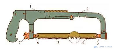
The diamond wire reciprocates on the fixed crystal, thereby cutting.
Like diamond tools, the diamond wire is not a simple piece of diamond. Diamond wire is processed on the basis of high-carbon steel wire, forming diamond serrations on the surface. The mainstream now is to introduce diamond particles, instead of directly synthesizing diamond on the surface. According to the different surface treatment methods, there are four types of diamond wires as follows:
1. Electroplated diamond wire: fix Ni and diamond particles on high carbon steel wire by electroplating;
2. Resin diamond wire: fix diamond particles on high carbon steel wire by heating phenolic resin and additives;
3. Inlaid diamond wire: fix the diamond particles on the high carbon steel wire by rolling;
4. Brazing diamond wire: the diamond particles are fixed on the high carbon steel wire by alloy brazing.
The resin diamond wire can get a better surface than the electroplated diamond wire, but the processing speed is slower.
| Cutting method | Principle | Incision/μm | Damage layer/μm | TTV/μm | Cutting speed mm/min |
| Electroplated diamond wire cutting | Carving | 80-120 | 6-8 | 8 | 1.35 |
| Resin diamond wire cutting | Carving | 80-120 | 4-7 | 5 | 0.9 |
| Mortar cutting | Grinding | 120-150 | 11-15 | 24 | 0.39 |
The cutting surface of silicon carbide ingots comparison is shown in the figure:
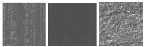
Separately show the surface of electroplated diamond wire cutting, resin diamond wire cutting, mortar cutting
1. Wire EDM for Cutting Silicon Carbide Ingots with Current-conducting
The material processed by the wire EDM should be able to conduct electricity. When the processed material is not conductive, the diamond wire cutting machine begins to show its processing advantages. It can cut conductive and non-conductive materials, as long as the hardness is less than the diamond wire.
2. Mortar cutting for Cutting Silicon Carbide Boules
Diamond wire cutting can be modified from mortar cutting.
The basic difference between diamond wire cutting and mortar cutting: the diamond wire cutting is cut by fixed diamond serrations on the line, while mortar cutting is grinding and cutting by silicon carbide particles or diamond particles in the mortar under the on-line extrusion. Because the mortar is fluid, the cut marks are often larger and the quality of cut surface is poor.
3. Laser cutting More Suitable for Cutting Silicon Carbide Wafers
The scheme of laser cutting silicon carbide is laser modified cutting technology. The principle is to use a laser beam with a high transmission wavelength to focus on the inside of the wafer through a lens, and multiphoton absorption occurs, resulting in a local deformation layer, namely modified layer. The layer is mainly composed of holes, high dislocation density layers and cracks. The modified layer is the starting point of subsequent wafer dicing and cracking. The modified layer can be confined inside the wafer by optimizing the laser and optical path system, and no thermal damage is caused to the surface and bottom of the wafer. Then, use external force to guide the cracks to the surface and bottom of the wafer, separating the wafer into the required size.
However, laser modified cutting requires a small thickness, which is suitable for silicon carbide wafer processing, while diamond wire cutting is used for silicon carbide ingots. Traditional wafer dicing usually uses a cutter wheel. The cutter wheel mainly grinds the wafer through its stable and high-speed rotation. During the cutting process, a coolant is used to reduce the temperature and remove debris. For wafers, laser modified cutting replaces the cutter wheel cutting. Laser modified cutting does not require coolant. There is no dust, and the cut marks are small. The speed can reach 1000 mm/s, and no blade consumables. The lifetime of laser is up to 30,000 hours, and the debugging time is less than 10 minutes. The specific cutting efficiency takes PAM-XIAMEN 4 inch 360 um SiC wafer, dia 2×2 mm as an example, it only takes 5 minutes.
In order to obtain the 4H-SiC wafer with low defects, the silicon carbide wafer usually needs to be grown on the seed crystal with 4° off-axis. Therefore, when the laser modified cutting is perpendicular to the flat side of the wafer, the crack will produce a 4° off-angle with the C-plane axis [0001]. When using ordinary laser cutting equipment for cutting, a 4° deflection angle will make it difficult to split the material, which will eventually cause severe chipping and meandering in this direction. More detailed control of the direction and energy of the laser is required.
Laser and tool cutting can be combined to form micro laser assisted precision cutting. Use laser heat to soften the surface of the workpiece, which can make the laser cutting silicon carbide easier and better. This processing technology is suitable for ultra-precision processing of materials, such as infrared crystals, cemented carbide, stainless steel, and glass.

For more information, please contact us email at victorchan@powerwaywafer.com and powerwaymaterial@gmail.com.