The structures of InxGa1-xAsyP1-y (indium gallium arsenide phosphide) quantum well epitaxially grown on InP substrate can be purchased or customized from PAM-XIAMEN. By adjusting the composition of x and y, the coverage wavelength range is from 870nm (GaAs) to 3.5um (InAs), which includes the optical fiber communication wavelengths of 1.3um and 1.55um. The 1.3 and 1.55um semiconductor light sources for optical fiber communication mainly use InGaAsP quantum well materials. This compound material can be used in photonic devices. More details a for InP wafers along with some epitaxial growth on top are listed below:
1. Structures based on InGaAsP Quantum Well (PAM170109-IGP)
Structure 1: InGaAsP/InP Epistacks
| InP | Substrate n-type, highly S-doped (1018cm−3) | |
| InP | SCH material, lightly doped or undoped | |
| hsch | Height of InP SCH layer (both sides) | 200 nm |
| In1−xGax Asy P1−y | QW Material | |
| x | Ga Fraction 0.25% compressive strain | – |
| y | As Fraction 0.25% compressive strain | – |
| Quantum Well Eg | Gap Energy of InGaAsP | – |
| hqw | Embedded InGaAsP QW height | 5nm |
| InP | Highly doped top ohmic contact p-type (1018cm−3) | |
| htop | Height of top ohmic contact | – |
Structure 2: Epitaxial In1−xGax Asy P1−y Growth on InP
| InP | Substrate n-type, highly S-doped (1018cm−3) | |
| InP | SCH material, lightly doped or undoped | |
| hsch | Height of InP SCH layer (both sides) | – |
| In1−xGax Asy P1−y | QW Material | |
| x | Ga Fraction 0.25% compressive strain | – |
| y | As Fraction 0.25% compressive strain | – |
| Quantum Well Eg | Gap Energy of InGaAsP | – |
| hqw | Embedded InGaAsP QW height | 4nm |
| InP | Highly doped top ohmic contact p-type (1018cm−3) | |
| htop | Height of top ohmic contact | 500 nm |
Structure 3: InP- based InGaAsP QWs
| InP | Substrate n-type, highly S-doped (1018cm−3) | |
| In1−xGax Asy P1−y | SCH material | |
| x | SCH Ga Fraction lattice matched | – |
| y | SCH As Fraction lattice matched | – |
| SCH Eg | SCH Gap Energy of InGaAsP | 1 eV |
| hsch | Height of InGaAsP SCH layer (both sides) | – |
| In1−xGax Asy P1−y | QW Material | |
| x | Ga Fraction 0.25% compressive strain | – |
| y | As Fraction 0.25% compressive strain | – |
| Quantum Well Eg | Gap Energy of InGaAsP | – |
| hqw | Embedded InGaAsP QW height | 5 nm |
| InP | Highly doped top ohmic contact p-type (1018cm−3) | |
| htop | Height of top ohmic contact | – |
Note:
There are not many layers: an SCH layer of InP, a narrow GaxIn1-xAsyP1-y quantum well, a second SCH layer of InP, and a heavily doped InP top layer for ohmic contact.
The second design is the same as the first, but thickness of the InGaAsP QW are different.
The third and last design is replacing the InP SCH layer with InGaAsP with a different fraction. Otherwise, everything else should be the same as design 1.
2. About Indium Gallium Arsenide Phosphide Properties
InxGa1-xAsyP1-y is quaternary solid solution with a narrow band gap. The following figure shows the relationship between refractive index n and wavelength for different composition InGaAsP lattice matched to InP at 300K:
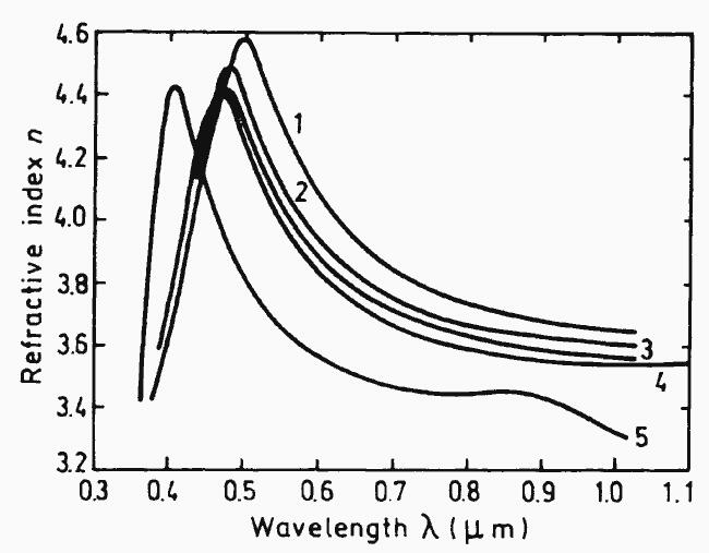
Refractive index n versus wavelength for different composition alloys lattice-matched to InP. 300 K
The relation for GaxIn1-xAsyP1-y refractive index n versus photon energy at 300 K is shown as the diagram:

Refractive index n versus photon energy for different composition alloys lattice-matched to InP. 300 K.
3. About GaxIn1-xAsyP1-y Material
Generally speaking, InGaAsP belongs to quaternary system, which is composed of indium arsenide, indium phosphide, gallium arsenide and gallium phosphide.
InGaAsP quantum wells (QW), including the single-quantum well and multi-quantum well can be grown by low pressure MOCVD on InP substrate. And the quantum well is grown with a InGaAsP composition of 1.3- um and 1.5- um, with InP barrier. For different structures, the indium gallium arsenide phosphide QW layer thickness is changing from 18 to 1300Å. The structures are analyzed by low temperature photo luminescence, showing an obvious, sharp luminous peak and the half widths of 4.8-1.3 meV.
GaxIn1-xAsyP1-y materials mainly emit light from free excitons. At room temperature, the carrier emission relaxation time of indium gallium arsenide phosphide materials reaches 10.4 ns, and it increases with the increase of excitation power.
The photonic ICs or PICs fabricated on InP material usually adopt GaxIn1-xAsyP1-y alloy to make the quantum well structure, waveguide and other photonic structures. The InGaAsP lattice constant is matched to InP substrate, making epitaxial thin film possible to grown on InP wafer. The GaxIn1-xAsyP1-y quantum well is almost used as an optical component (like photodetector and modulator) in C band communications as well as the 1.55um near infrared devices.

For more information, please contact us email at victorchan@powerwaywafer.com and powerwaymaterial@gmail.com.