InGaP / GaAs heterojunction bipolar transistor (HBT) has become one of the highly competitive and promising high-speed solid-state devices in the current microwave and millimeter wave field due to its high reliability, low cost, and relatively mature technology. PAM-XIAMEN provide InGaP / GaAs HBT wafers. And we grow InGaP as the emitter material in the GaAs HBT structure. The yield of HBT devices can be improved since a good selective corrosion can be achieved between InGaP and GaAs. Detailed HBT device wafer specification please refer to the table below:
1. InGaP / GaAs HBT Epi Wafer
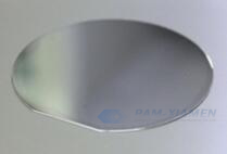
PAM210709 – HBT
| Layer Name | Epi Material | Thickness | Dopant | Doping Concentration |
| Contact Layers | InGaAs | – | ||
| GaAs | – | |||
| Emitter Layer | Ga0.51In0.49P | – | n | – |
| Base Layer | GaAs | – | p | 4×1019 cm-3 |
| Collector Layer | GaAs | – | n | – |
| Subcollector Layer | GaAs | 700nm | n | – |
| Substrate | GaAs |
2. What Is Heterojunction Bipolar Transistor?
Heterojunction bipolar transistor (HBT) is a kind of bipolar transistor, whose emission region and base region use different semiconductor materials. In this way, the emission junction (i.e. the PN junction between the emission region and the base region) forms a heterojunction. The HBT has better high-frequency signal characteristics and base emission efficiency than the general bipolar transistor, and can work under signals up to hundreds of GHz. It is widely used in modern high-speed circuits, RF systems, and mobile phones.
Heterojunctions in semiconductors are a special type of PN junction formed by the deposition of two or more thin films of different semiconductor materials on the same substrate. These materials have different energy band gaps, which can be compounds such as GaAs or semiconductor alloys such as silicon germanium. Among numerous heterogeneous material systems, epitaxial growth of InGaP / GaAs material can improve the current gain, reliability, stability, and yield of HBT devices, making it still the most competitive material system among microwave devices at present.
3. Effects of Degree of Order in InGaP Materials on GaAs HBT Wafer
The degree of ordering of InGaP materials mainly affects their properties in the following aspects:
a) The band gap of GaInP ordered structure is smaller than that of disordered structure.
b) The antiphase boundaries in ordered InGaP materials may become the composite center, which will not occur in disordered InGaP.
c) In the InGaP / GaAs HBT material system, the conduction band discontinuity △Ec between ordered InGaP materials and GaAs is very small, while semi ordered InGaP and GaAs have relatively large △Ec. So for GaAs HBT process, we tend to grow semi ordered InGaP. Compared with ordered InGaP epitaxial layers, semi ordered InGaP epitaxial layers have fewer recombination centers.
d) The degree of order in the HBT structure will affect the distribution of △Ec and △Ev at the heterojunction. The reported △Ec in the literature ranges from 0.03eV to 0.39eV, which may be due to differences in ordering.
Remark:
The Chinese government has announced new limits on the exportation of Gallium materials (such as GaAs, GaN, Ga2O3, GaP, InGaAs, and GaSb) and Germanium materials used to make semiconductor chips. Starting from August 1, 2023, exporting these materials is only allowed if we obtains a license from the Chinese Ministry of Commerce. Hope for your understanding and cooperation!

For more information, please contact us email at victorchan@powerwaywafer.com and powerwaymaterial@gmail.com.