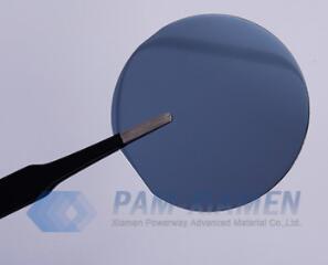
PAM-XIAMEN can offer AlGaAs / GaAs p-HEMT (pseudomorphic high electron mobility transistor) heterostructure epitaxial wafer grown by MBE or MOCVD process. The heterostructure has a high-mobility conduction channel formed by two-dimensional electron gas, which is an ideal material for wireless applications. The line width of our GaAs pHEMT process is about 0.15-0.5μm, very low but with ultra-high frequency and low noise characteristics and the operating frequency can be as high as 100GHz. The specific specifications of GaAs pHEMT epiaxy wafer are as follows, we can also provide customized GaAs epi-wafers:
1. GaAs pHEMT Wafer Specifications
No. 1 LN pHEMT Epi Structure (PAM160711-GAAS)
| Layer | Material | x | Dopant | Concentration | Thickness (A) | Remarks |
| 12 | n+-GaAs | – | Si | 5.0E+18 cm-3 | 500 | – |
| 11 | n-AlAs | – | Si | – | – | – |
| 10 | n-AlxGa1-xAs | 0.22 | Si | – | – | – |
| 9 | Si | – | Si | 5.0E+12 cm-2 | – | – |
| 8 | AlxGa1-xAs | 0.22 | – | – | 30 | – |
| 7 | InxGa1-xAs | – | – | – | – | – |
| 6 | GaAs | – | – | – | – | – |
| 5 | AlAs | – | – | – | – | – |
| 4 | GaAs | – | – | – | – | – |
| 3 | AlAs | – | – | – | – | – |
| 2 | AlxGa1-xAs/GaAs | 0.22 | – | – | 185/15 | 10 X SLs |
| 1 | GaAs | – | – | – | 5000 | – |
| S.I. GaAs Substrate | ||||||
No.2 Power pHEMT Epitxial Structure (PAM160711-GAAS)
| Layer | Material | x | Dopant | Concentration | Thickness (A) | Remarks |
| 13 | n+-GaAs | – | Si | – | 500 | – |
| 12 | n-AlAs | – | – | – | – | – |
| 11 | GaAs | – | – | – | – | |
| 10 | n-AlxGa1-xAs | 0.24 | Si | – | – | – |
| 9 | Si | – | Si | 3.0E+12 cm-2 | – | – |
| 8 | AlxGa1-xAs | – | – | – | 25 | – |
| 7 | InxGa1-xAs | – | – | – | – | – |
| 6 | AlxGa1-xAs | – | – | – | 30 | – |
| 5 | Si | – | Si | 1.0E+12 cm-2 | – | – |
| 4 | AlxGa1-xAs | – | – | – | – | – |
| 3 | GaAs | – | – | – | – | – |
| 2 | AlxGa1-xAs | 0.24 | – | – | – | – |
| 1 | GaAs | – | – | – | – | – |
| S.I. GaAs Substrate | ||||||
No.3 GaAs Epi Wafers for pHEMTs (PAM161121-PHEMT)
| Layer material with doping | Thickness (A) | Doping level | Composition | Note |
| n+-GaAs | 400 | – | – | – |
| AlAs | – | – | – | – |
| GaAs | – | – | – | – |
| n-AIGaAs | – | 3E+17cm-3 | – | – |
| GaAs | 9 | – | – | – |
| Si | – | – | – | – |
| GaAs | – | – | – | – |
| i-AIGaAs | – | – | – | Spacer |
| i-GaAs | – | – | – | – |
| i-InGaAs | – | – | – | – |
| i-GaAs | – | – | – | – |
| i-AIGaAs | – | – | 0.24 | – |
| GaAs | – | – | – | |
| Si | – | 1.5E+12cm-2 | – | – |
| GaAs | 9 | – | – | – |
| i-AIGaAs | – | – | – | – |
| AIGaAs 100A/GaAs 20A superlattice 15 periods | – | – | – | – |
| i-GaAs | – | less than 5E+14cm-3 | – | – |
| S.I. GaAs substrate |
We also can provide InP-based pHEMT epitaxial wafer:
PAM160526-INP
| Layer | Material | Concentration | Thickness |
| 8 | N+ InxGa1-xAs | – | 20nm |
| 7 | N+ InP etch stopper | – | – |
| 6 | i-InxAl1-xAs Schottky barrier | – | – |
| 5 | Si-delta-doping | n=6×1012 cm-2 | – |
| 4 | i-InxAl1-xAs spacer | – | – |
| 3 | i-InxGa1-xAs channel | – | – |
| 2 | InxAl1-x As buffer | – | 300nm |
| 1 | metamorphic buffer (linearly graded from substrate to
InxGa1-x As) |
– | – |
| InP substrate |
In recent years, with the popularization and application of mobile communication and wireless Internet systems, a strong demand for semiconductor device products has been stimulated. Semiconductor epitaxial materials are an important foundation for devices used in wireless communications. In order to meet the market’s requirements for product quality and cost, it is very important to develop a high-capacity and stable process. GaAs pHEMT has excellent performance in the leader of wireless applications, and has moved towards mass production. Therefore, the development of an efficient epitaxial process plays an important role in reducing costs and market response time. Molecular beam epitaxy (MBE) is the main technical method for growing GaAs pHEMT epitaxial materials. Compared with other growth methods, such as metal organic chemical vapor deposition (MOCVD), MBE has higher control accuracy and stability.
2. About GaAs pHEMT Epitaxial Material
The 2-DEG in pHEMT is more restricted than the ordinary HEMT: there is a double restriction on both sides of the potential well, so it has a higher electron surface density (about 2 times higher). At the same time, the electron mobility is also higher than that in GaAs. Therefore, the performance of pHEMT is more superior. Double heterojunction GaAs pHEMT epitaxial structure not only improves the temperature stability of the threshold voltage of the device, but also improves the output volt-ampere characteristics of the device, so that the device has a larger output resistance, a higher transconductance, and a larger current handling capacity and higher operating frequency, lower noise and so on.
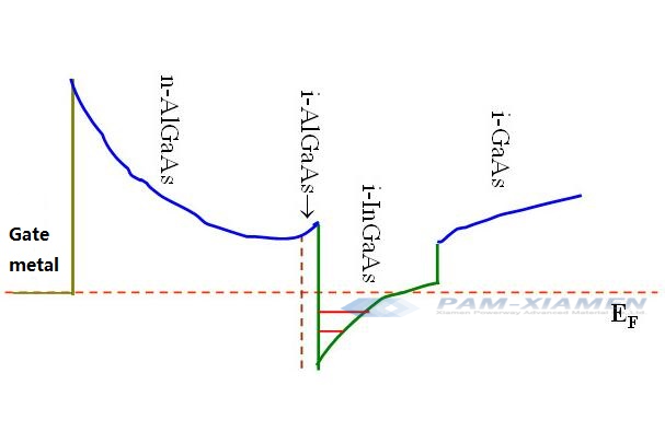
Energy Band Diagram of pHEMT Heterojunction
The channel mobility of GaAs pHEMT epitaxial materials is one of the most important indicators. Increasing the channel mobility can effectively improve the DC and RF performance of gallium arsenide pHEMT products (such as GaAs pHEMT transistor, GaAs pHEMT amplifier and MMIC), which has great effects on application parameters such as transconductance, on-state resistance, cut-off frequency, noise figure, RF gain, and power conversion efficiency.
3. About GaAs pHEMT
pHEMT is an improved structure of high electron mobility transistor (HEMT), also known as pseudo-matched high electron mobility transistors (pHEMT), which is a radio frequency GaAs power transistor made using a special epitaxial layer grown on GaAs can achieve low voltage and high efficiency when used in cellular phones and radio frequency modems.
GaAs pHEMT application is in microwave and millimeter wave frequency bands due to the excellent properties of high electron mobility, high current modulation efficiency, and low loss. As the operating frequency of the device enters the millimeter wave frequency band, the influence of parasitic effects on the performance of the device becomes very obvious. Model is the basis of circuit design, and the method of accurately extracting model parameters of transistor high-frequency parasitic effects has always been a research hotspot in the industry.
With the continuous development of 5G wireless communication components and infrastructure, GaAs pHEMT technology will play a key role to meet the multiple characteristics of new wireless networks. In the development of 5G key components, we continue to improve our GaAs pHEMT process flow to provide a full range of related products in linear digital radios, V-band, E-band and W-band radar applications.

For more information, please contact us email at victorchan@powerwaywafer.com and powerwaymaterial@gmail.com.