Indium antimonide (InSb) detector is sensitive for the mid-wave infrared (MWIR) band. In terms of mid-infrared detection in the 3-5um band, due to the advantages of mature material technology, high sensitivity and good stability, InSb detectors stand out from detectors based on other materials. At low temperature, InSb material has a high absorption coefficient for infrared light (~1014cm-1), a quantum efficiency greater than or equal to 80%, and a high carrier mobility (un~105cm2∙V-1∙s-1). InSb IR detector has very prominent technical advantages, and its application fields cover precision guidance, portable imaging, vehicle, shipborne, airborne, aerospace, etc. InSb detector array offered by PAM-XIAMEN is 128 x 128 pixels, and detector spectral response range is 3.7 um~4.8 um. Specifications please refer to table below:
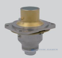
1. Technical Parameters of MWIR InSb Detector
| Product Name | Main Specification | |
| MW128×128
(J-T) InSb Infrared Detector |
Number of Pixels | 128×128 |
| Pixel Pitch | 15um×15um | |
| Pixel Operability | 99% | |
| Responsivity Non-uniformity | ≤6% | |
| NETD | ≤15mK | |
| FOV | 2 | |
| Cooldown Time | ≤30s | |
| Weight | ≤250g | |
2. Process of Infrared InSb Detectors
With the continuous development of infrared detection technology, photosensitive chips based on InSb materials have gone through from unit chips to multi-element, line array, and area array chips. After the flip-chip interconnection process, the photosensitive chip and the signal processing circuit are combined together and placed on the focal plane of the optical system, which constitutes the core component of infrared signal detection. In the realization of photoelectric conversion, the performance of the photosensitive chip is one of the key factors that determine the detection level of the cooled InSb detector. In the preparation of the area array photosensitive chip, the quality of the PN junction and the effective isolation of the photosensitive pixel units are the core keys to the preparation of the area array chip. The preparation process of PN junction is divided into diffusion process, ion implantation process and epitaxy process. For different PN junction fabrication techniques, the corresponding surface array structure fabrication techniques are also different.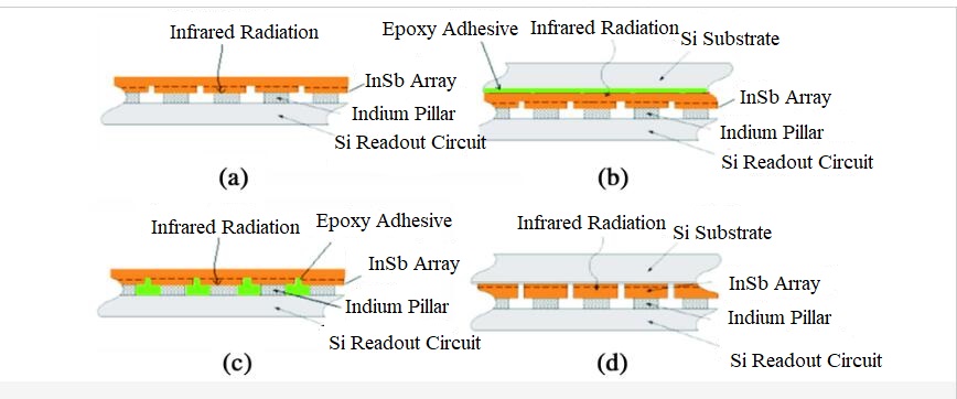
Schematic Diagram of InSb Focal Plane Detector Technology Route
The technical level of infrared InSb detector in the medium wave band has been continuously improved. The size of the area array continues to increase, the InSb detector quantum efficiency continues to improve, and the high-temperature operation and dual multi-color detectors are fully developed.

For more information, please contact us email at victorchan@powerwaywafer.com and powerwaymaterial@gmail.com.