Compared to 4H-SiC, although the bandgap of 3C silicon carbide (3C SiC) is lower, its carrier mobility, thermal conductivity, and mechanical properties are better than those of 4H-SiC. Moreover, the defect density at the interface between the insulating oxide gate and 3C-SiC is lower, which is more conducive to manufacturing high-voltage, highly reliable, and long-life devices. At present, 3C-SiC based devices are mainly prepared on Si substrates. The large lattice mismatch and thermal expansion coefficient mismatch between Si and 3C SiC result in a high defect density, which affects the performance of devices. Moreover, low-cost 3C-SiC wafer will have a significant substitution impact on the power device market in the 600V-1200V voltage range, accelerating the entire industry’s progress. Therefore, developing bulk 3C-SiC wafer is inevitable.
PAM-XIAMEN can produce bulk 3C-SiC wafer in N type, with a higher electron mobility (3C SiC: 1100 cm2/V·s; 4H SiC:900 cm2/V·s). Since 3C-SiC bandgap width is smaller, the device can have a smaller FN tunneling current and reliability in oxide layer preparation, which can significantly improve the yield of the device. Additional information of 3C-SiC wafer, please refer to the parameters’ sheets below:
1. 3C SiC Wafer Specifications
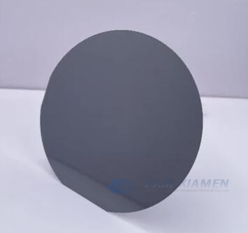
No. 1 50.8mm 3C-SiC Substrate
| Item | 2 inch N-Type 3C-SiC Substrate | |||
| Grade | Ultra-Prime Grade | Industrial Grade | Test Grade | |
| Diameter | 50.8±0.38mm | |||
| Thickness | 350±25um | |||
| Conductivity | N | |||
| Orientation | on axis:<0001>±0.5° | |||
| Primary Flat Orientation | {1-10}±5.0° | |||
| Primary Flat Length | 15.9±1.7mm | |||
| Secondary Flat Orientation | Si face up: 90° CW.from prime flat ±5.0° | |||
| Secondary Flat Length | 8.0±1.7mm | |||
| MPD* | <0.1 cm-2 | |||
| Resistivity* | ≤0.8Ω·cm | ≤1Ω·cm | ||
| LTV | ≤2.5μm | |||
| TTV | ≤5μm | |||
| Bow | ≤15μm | |||
| Warp | ≤25μm | ≤30μm | ||
| Roughness* | Polishing | Ra≤1nm | ||
| CMP | Ra≤0.2nm | Ra≤0.5nm | ||
| Edge Cracks by High Intensity Light | None | 1 allowed, ≤1mm | ||
| Hex Plates by High Intensity Light* | Cumulative area≤0.05% | Cumulative area≤3% | ||
| Polytype Areas by High Intensity Light* | None | Cumulative area≤5% | ||
| Visual Carbon Inclusions | Cumulative area≤0.05% | Cumulative area≤3% | ||
| Scratches on Si Face by High Intensity Light | None | 8 scratches to 1x wafer diameter cumulative length | ||
| Edge Chips by High Intensity Light | None permitted≥0.2mm width and depth | 5 allowed, ≤1mm each | ||
| Si-Face Contamination by High Intensity Light | None | |||
| Edge Exclusion | 1mm | 5mm | ||
| Package | Single Wafer Box or Multi Wafer Box | |||
“*” value is applicable to the entire wafer surface except for edge exclusion areas
No. 2 100mm 3C-SiC Substrate
| Item | 4 inch N-Type 3C-SiC Substrate | |||
| Grade | Ultra-Prime Grade | Industrial Grade | Test Grade | |
| Diameter | 99.5~100mm | |||
| Thickness | 350±25um | |||
| Conductivity | N | |||
| Orientation | on axis{111}±0.5° | |||
| Primary Flat Orientation | {1-10}±5.0° | |||
| Primary Flat Length | 32.5±2.0mm | |||
| Secondary Flat Orientation | Si face up: 90° CW.from prime flat ±5.0° | |||
| Secondary Flat Length | 18.0±2.0mm | |||
| MPD* | <0.1 cm-2 | |||
| Resistivity* | ≤0.1Ω·cm | ≤0.3Ω·cm | ||
| LTV | ≤2.5μm | ≤10μm | ||
| TTV | ≤5μm | ≤15μm | ||
| Bow | ≤15μm | ≤25μm | ||
| Warp | ≤30μm | ≤40μm | ||
| Roughness* | Polishing | Ra≤1nm | ||
| CMP | Ra≤0.2nm | Ra≤0.5nm | ||
| Edge Cracks by High Intensity Light | None | Cumulative length≤10mm,single length≤2mm | ||
| Hex Plates by High Intensity Light* | Cumulative area≤0.05% | Cumulative area≤0.1% | ||
| Polytype Areas by High Intensity Light* | None | Cumulative area≤3% | ||
| Visual Carbon Inclusions | Cumulative area≤0.05% | Cumulative area≤3% | ||
| Scratches on Si Face by High Intensity Light | None | Cumulative≤1 x wafer diameter | ||
| Edge Chips by High Intensity Light | None permitted≥0.2mm width and depth | 5 allowed, ≤1mm each | ||
| Si-Face Contamination by High Intensity Light | None | |||
| Edge Exclusion | 3mm | 6mm | ||
| Package | Single Wafer Box or Multi Wafer Box | |||
“*” value is applicable to the entire wafer surface except for edge exclusion areas
2. Superiority of 3C-SiC Analyzed Based on MOSFET Device
Firstly, the electron mobility (view table 1). According to reports, the n-channel mobility range of silicon-based 3C SiC MOSFETs is 100-370 cm2/V·s. The lateral 4H-SiC MOSFET is usually 20-40 cm2/V·s, and the groove device is 6-90 cm2/V·s. The SiC MOSFETs have been created on the A-side through nitrogen passivation, increasing the channel mobility to 131 cm2/V·s, but also lower than silicon-based 3C SiC devices.
| Table 1 Properties of Cubic Silicon Carbide (3C-SiC) Compared to Other Semiconductor Materials (@300K) | ||||||||
| Material | Bandgap (eV) | Intrinsic Carrier Conc. (cm-3) | Dielectric Constant | Electron Mobility (cm2/Vs) | Critical Electric Field (MV/cm) | Saturation Velocity (107cm/s) | Thermal Conductivity (W/cmK) | Baliga Figure of Merit |
| 3C-SiC | 2.36 | 1.5×10⁻¹ | 9.7 | 800 | 1.4 | 2.5 | 3.2 | 86 |
| 4H-SiC | 3.26 | 8.26×10⁻⁹ | 10 | 720a
650c |
2.8 | 2.0 | 4.5 | 556 |
| Si | 1.12 | 1.5×10¹⁰ | 11.8 | 1350 | 0.2 | 1.0 | 1.5 | 1 |
| Diamond | 5.45 | 1.6×10⁻²⁷ | 5.5 | 3800 | 10 | 2.7 | 22 | 8.4×10⁴ |
| 2H-GaN | 3.39 | 1.9×10⁻¹⁰ | 9.9 | 1000a
2000** |
3.75a
3.3* |
2.5 | 1.3 | 3175 |
| GaAs | 1.42 | 1.8×10⁶ | 13.1 | 8500 | 0.4 | 1.2 | 0.55 | 29 |
Next is reliability. Currently, the core technology bottleneck of SiC MOSFET is concentrated in the poor interface quality of the gate oxide layer, which not only has low channel mobility but also affects the stability of the threshold voltage. The gate oxide also has a weakness of failure at high temperatures. The interface trap concentration between 3C-SiC and insulating oxide gate is much lower, which helps to manufacture reliable and long-life devices.
Besides, the barrier height of 3C-SiC is 3.7 eV (view Fig.1), which is much higher than that of silicon and 4H SiC. Therefore, when the leakage current in the gate drive circuit is the same, the electric field inside 3C-SiC MOSFET is two to three times higher than that in 4H-SiC. Therefore, the derating requirements for 3C-SiC trench power MOSFETs are far less stringent than those for 4H-SiC devices.
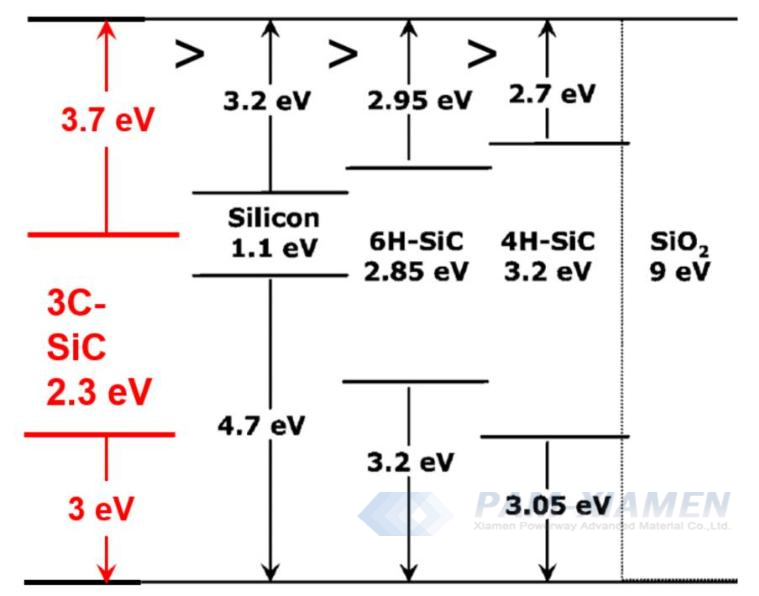
Fig.1 Band Structure of Main Power Semiconductor on 3C-SiC, 4H-SiC, 6H-SiC and Silicon (illustrating band offsets with SiO2)
Last but not least, 3C-SiC with low energy bandgap width is closer to silicon, which has many benefits when processed into devices.
3. Differences of 4H-SiC, 6H-SiC, 3C-SiC in Applications
4H-SiC has high electron mobility, low conduction resistance, and high current density, making it suitable for power electronic devices.
6H-SiC has a stable structure and good luminescence performance, making it suitable for optoelectronic devices.
3C-SiC has a high saturation electron drift velocity and a thermal conductivity second only to diamond single crystals, making it suitable for high-frequency and high-power devices.

For more information, please contact us email at victorchan@powerwaywafer.com and powerwaymaterial@gmail.com.