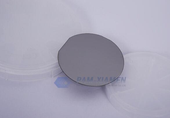
GaSb (Gallium Antimonide) crystal substrate is available with P type or N type in various sizes. The minimum value of GaSb substrate mobility can reach 200 cm2/V.s, and the maximum can reach 3500 cm2/V.s. PAM-XIAMEN’s gallium antimonide semiconductor material is a single crystal grown by a special LEC method. It is used in infrared detectors, infrared light-emitting diodes (LED), lasers, converters, thermostat photoelectric systems, etc. The main parameters are listed as follows:
1. Main Parameters of Single Crystal GaSb Substrate
| Main Parameters | |||||||
| Single crystal | Dopant | Conductivity type | Carrier concentration | Mobility (cm2/V.s) |
Dislocation density(cm-2) | Standard substrate | |
| cm-3 | |||||||
| GaSb | / | P | (1-2)*10^17 | 600-700 | <1*10^4 | Φ2″×0.5mm | |
| Φ3″×0.5mm | |||||||
| GaSb | Zn | P | (5-100)*10^17 | 200-500 | <1*10^4 | Φ2″×0.5mm | |
| Φ3″×0.5mm | |||||||
| GaSb | Te | N | (1-20)´10^17 | 2000-3500 | <1*10^4 | Φ2″×0.5mm | |
| Φ3″×0.5mm | |||||||
| dimension (mm) | Diameter 50.8×0.5mm, 10×10×0.5mm, 10×5×0.5mm | ||||||
| Surface roughness | Surface roughness(Ra): <= 5A | ||||||
| Polishing | One side or double side polished | ||||||
2. Surface Treatment for GaSb Single Crystal Substrate
For the gallium antimonide substrate, the first problem to be solved is the removal of gallium antimonide oxidation state. Since there are no Ga and Sb sources in the usual Hg-MBE equipment, the pretreatment of the GaSb substrate needs to be carried out in a III-V family chamber, and then transferred to the Hg-MBE for HgCdSe material epitaxy. The method is to first heat the substrate to about 590°C to remove the oxide layer in the III-V chamber. After the removal, the substrate temperature is reduced to about 500°C to grow a layer of GaSb with a thickness of about 0.2 microns. In this way, a clean and flat GaSb surface suitable for HgCdSe epitaxy can be obtained. In order to prevent the GaSb surface from being oxidized again during the transfer of the substrate to the II-VI chamber, a layer of As is grown on the surface of the substrate again after the growth of GaSb is completed and before the substrate drops to room temperature. After entering the II-VI chamber, the As layer on the surface is removed by heating the substrate. It should be noted in the process that the temperature and heating time for gallium antimonide wafers need to be strictly controlled to ensure that As and O are completely removed, and the GaSb wafer surface has a good composition ratio.
At present, the surface treatment technology of GaSb substrates is not ideal. Regardless of the relatively mature GaSb (100) or GaSb (211) substrate, there will be small pits of about 20nm on the surface, which are mainly generated during the grinding and polishing process of the gallium antimonide single crystal substrate surface. Although the half-width of X-ray double crystal diffraction is generally about 20 and 30 aresec respectively, it is best to reach 18 aresec. Furthermore, the surface roughness and small pits will affect the quality of the epitaxial layer.
3. GaSb Semiconductor Material Development
Gallium antimonide crystals have a good development prospect in the field of infrared detection and laser. The second-class superlattice structure infrared detector developed with GaSb as the substrate has excellent performance and has important applications in the mid-infrared band, such as production multi-purpose infrared detectors and sensors for fire alarms and environmental pollution detection. At the same time, GaSb substrate can also be used to prepare light emitting devices in the 2-5um band, which are used in various engineering fields such as optical communications, lasers, and photosensitive detection.

For more information, please contact us email at victorchan@powerwaywafer.com and powerwaymaterial@gmail.com.