The PN junction material has a single conductivity, which is a characteristic utilized by many devices in electronic technology, such as semiconductor diodes and bipolar transistors. PAM-XIAMEN can offer silicon PN junction wafers. Here we just list a specific epitaxial structure of photodiode application for your reference. More silicon epitaxial wafers please refer to https://www.powerwaywafer.com/silicon-wafer/epitaxial-silicon-wafer.html.
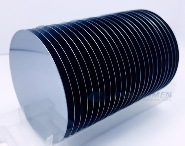
1. Silicon P-N Junction Wafer Specification
PAMP21452 – PN
| Substrate | Silicon |
| Diameter | 5inches |
| Type | P |
| Thickness | 500um |
| Surface Finished | One side polished |
| Ro | 8-12Ω·cm |
| Epi layer | Silicon |
| Type | N |
| Ro | 8Ω·cm |
| Thickness | 15um |
2. What Is A Silicon PN Junction?
By doping ion implantation, diffusing dopants, or epitaxial growth, P-type semiconductors and N-type semiconductors are fabricated on the same silicon substrate, forming a space charge region called a silicon P-N junction at their interface. P-N junction is a device used for rectification, switching, and other purposes, as well as the basic structure of semiconductor microwave devices and optoelectronic devices. It is also a fundamental component of bipolar transistors, thyristor rectifiers, and field-effect transistors. The most important property of silicon junctions is the rectification effect, which allows only one direction of current to pass through.
PN junction for silicon even other materials can be roughly divided into two types:
(1) Mutant junction: The impurity concentration in the two zones of the PN junction is uniformly distributed, and impurity mutations occur at the interface. If the impurity concentration in one region is much higher than that in the other region, it is called a unilateral mutation junction P+N or N+P junction. Formed by alloy, shallow diffusion, or low energy ion implantation.
(2) Linear slowly changing junction: The impurity distribution near the junction is slowly changing, which can be approximated by a straight line, and its slope is called the impurity concentration gradient. A junction obtained by deep diffusion or high-energy ion implantation.
3. How PN Junction Works?
PN junctions are usually in two states that are cutoff state and forward bias state:
In the cut-off state, the difference in carrier concentration on both sides of the PN junction forms an electric field, which makes it difficult for free charges to pass through the PN junction when the applied voltage is zero;
When the applied voltage is positively biased, this electric field is weakened, and electrons quickly pass through the PN junction and generate current. When the applied voltage is reverse biased, this electric field strengthens, creating an effect that prevents the current from moving forward.
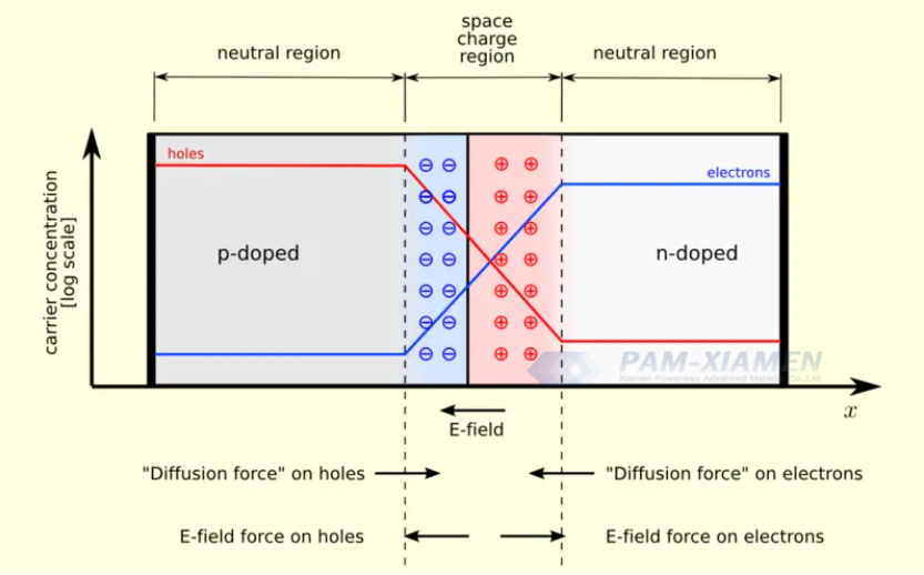
PN Junction Working Principle

For more information, please contact us email at victorchan@powerwaywafer.com and powerwaymaterial@gmail.com.