PAM-XIAMEN can supply SiC substrates with various specifications, please get more info from: https://www.powerwaywafer.com/sic-wafer/sic-wafer-substrate.html
1. Significance of Research on Correlation Between Defect Rate and Mechanical Strength
It is well known that SiC defects have great negative impact to the electrical reliability and performance of chips; Their impact on the mechanical yield of devices has not been properly studied. Therefore, it is useful to study the correlation between the defect rate (whether intrinsic or process induced) of 4H-SiC substrates and its mechanical strength. Bending strength, referring to the stress that the mold can withstand under the load applied at the time of fracture, has been used as a reference parameter. The three-point bending (3PB) test has been performed on identified substrate areas and collected data, which is correlated with the corresponding defect density.
2. Study of Defect Density on Mechanical Characteristics of 4H-SiC
This study conducted a control experiment using a 150 mm 4° off-angle 4H-SiC substrate:
One group of SiC substrates characterized by different dislocation densities (wafer # 1 and wafer # 2) was used to study the effect of inherent SiC defects on mechanical strength. Perform a 5 min KOH wet etching process at 500℃ to highlight SiC crystal defects. The optical inspection of the wafer surface after KOH etching has been carried out using an automatic optical microscope (nSPEC by Nanotronics) to monitor the density and distribution of defects. The entire chip was inspected using an x10 objective lens.
And another group of substrates underwent thinning treatment, followed by high-temperature bulk heat treatment and high-throughput laser treatment, to study the effect of process defects on mechanical strength.
A failure strength investigation was conducted on all wafers through a 3-point bending test (Instron 5566), and the correct selection was made based on the defect density on the wafers on various 5×4 mm molds. The tool accuracy is 0.5%, and the supporting span length is 3mm. The load is applied at the center of the span and increases at a constant rate of 0.5 mm/min.
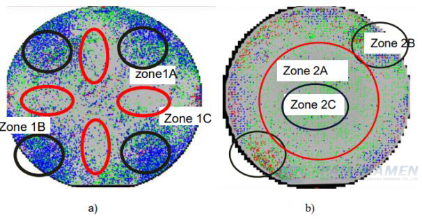
Fig. 1 Distribution of defect density at the wafer scale after KOH using n-spec analysis, with high and low density areas marked by black and red circles respectively. Etch wafer # 1 a) and wafer # 2 b).
In the experiment, it was found that BPD was mainly caused by stress caused by lattice distortion strain in both high-density and low-density areas investigated. In high-density areas, BPD array half ring array (HLA) was found.
Conduct a three-point bending test on the selected mold to calculate the stress that the mold can withstand when it fractures σ (Bending strength), according to the theory of suspension beams with known geometric shapes supported at both ends, can be expressed as: σ= 3FL/2Wd2.
In the formula, F is the maximum load, which causes the mold to fracture, and L, W, and d are the length, width, and thickness of the mold, respectively. In this experiment, the mold size is 5 × 4 millimeters and the mold thickness is 350 um. In areas with defect densities as high as 2000/mold size, no significant changes in mold strength were observed. It is worth noting that molds with low bending strength corresponding to low defect density account for 7% -10% of the total analyzed low-density molds.
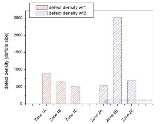
Fig. 2 Defect density as a function of each wafer # 1 (red) and wafer # 2 (blue) in the wafer region
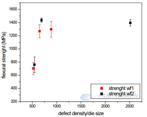
Fig. 3 Variation of bending strength of inherent defects with defect density
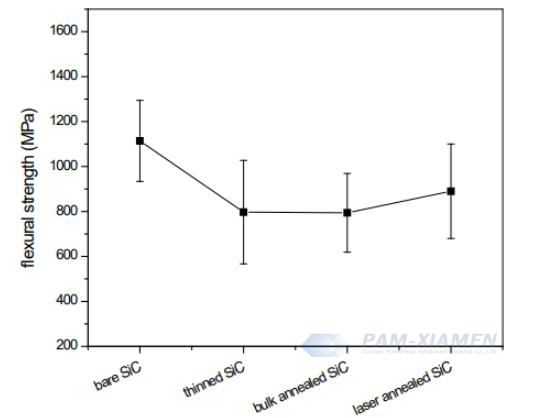
Fig. 4 Variation of bending strength as a function of defect density induces defects
The results indicate that within the range of high defect density in SiC crystals, the bending strength of the mold remains basically unchanged. However, the defect density generated during the thinning process on the SiC surface reduces the mold strength by 1.4 times, and this value remains almost unchanged under subsequent high-temperature treatment.

For more information, please contact us email at victorchan@powerwaywafer.com and powerwaymaterial@gmail.com.