PAM XIAMEN offers Pyrolytic Boron Nitride.
Performance PBN’s properties, its intrinsic purity, superior mechanical strength, and thermal stability make it a superb choice for high temperature furnace and electrical components; microwave and semiconductor components; and industry standardized crucibles for Gallium Arsenide Crystal production.
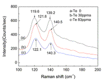
Good [...]
2019-05-14meta-author
PAM-XIAMEN can offer LED epitaxy wafers and is able to offer GaN foundry services & supplies for LEDs. The GaN foundry services include OEM growth service, COW process and various test services. Specifically as follows:
1. OEM Service – Customized AlGaN-based Thin Film Epi Structure
We [...]
2022-11-22meta-author
PAM XIAMEN offers (100) orientation Silicon Substrates.
Below is just a small selection. Let us know if you can use or if we can quote you on another spec.
Item
Material
Orient.
Diam
(mm)
Thck
(μm)
Surf.
Resistivity
Ωcm
Comment
PAM2929
n-type Si:P
[100]
4″
525
P/E
43657
SEMI Prime, 2Flats, Empak cst
PAM2930
n-type Si:P
[100]
4″
525
P/E
43657
SEMI Prime, 2Flats, Empak cst
PAM2931
n-type Si:P
[100]
4″
224
P/E
5–10
SEMI Flats (two), Empak cst, Cassette of [...]
2019-02-22meta-author
PAM-XIAMEN can offer 2&3 inches P-type GaAs substrates. Gallium arsenide (GaAs) is a III-V type direct band gap semiconductor with a zinc blend crystal structure, and GaAs p-type dopant is commonly used as a substrate for epitaxial growth of other III-V semiconductors, including indium gallium arsenide, aluminum gallium [...]
2021-04-15meta-author
Highlights
•Aberration-corrected TEM and EELS reveal structural and elemental profiles across GaAs/Si bond interfaces in wafer-bonded GaInP/GaAs/Si – multi-junction solar cells.
•Fluctuations in elemental concentration in nanometer-thick amorphous interface layers, including the disrubutions of light elements, are measured using EELS.
•The projected widths of the interface layers [...]
PAM XIAMEN offers Au (highly oriented polycrystalline)/Ti/SiO2/Si substrate: PAM-191005-SI/SIO2/TI/AU: Au( highly oriented polycrystalline)/Ti/ SiO2 on Silicon substrate ,4″x0.525 mm,1sp P-type B-doped, Au(111)=50 nm, Ti=2 nm ,SiO2=300nm
Specifications Au/Ti/SiO2/Si substrate:
1.Structure: Au/Ti/ SiO2 on Si substrate
Flim thickness:
Au(111)=50 nm
Ti=2 nm
SiO2=300 nm
2.Substrate spec:
Material:Si substrate
Size: 4″ dia.
Orientation:(100)
Type:P type
Dopant:B doped
Thickness:525 um
Grade: [...]
2019-04-26meta-author