P type GaAs(Gallium Arsenide) Wafer
PAM XIAMEN offers p type GaAs(100) Zn-doped crystal Wafer.
1.Wafer List:
GF-GaAs (100) orientation, Zn-doped 10x10x0.625 mm, single side polished.
GaAs Wafer – Growing Method: VGF (100) Zn doped P-type, , 2″x0.5 mm, single side polished, (1-5) x 10^19 /cm^3
GaAs Wafer – Growing Method: VGF (100) Zn doped P-type, , 2″x0.5 mm, double side polished, (1-5) x 10^19 /cm^3
GaAs Wafer – Growing Method: VGF (100) P type Zn doped , 3″x0.625 mm, single side polished
GaAs Wafer – Growing Method: VGF (100) Zn doped Ptype, , 2″x0.35 mm, single side polished, CC: (1-5) x 10^19 /cm^3
GaAs Wafer – Growing Method: VGF (100), Zn doped, P-Type, 3″x0.5 mm, single side polished
GaAs Wafer – Growing Method: VGF (100) Zn doped P-type , 100mm x0.625 mm, double side polished, Carrier Concentration:(1.00-1.94) x 10^19 /cm^3
GaAs Wafer – Growing Method: VGF (100) Zn doped P type, , 100mm x0.5 mm, single side polished, Carrier Concentration:(1-5) x 10^19 /cm^3
GaAs Wafer – Growing Method: VGF (100) Zn doped P-type , 150mm x0.625 mm, double side polished, Carrier Concentration:(1.00-1.94) x 10^19 /cm^3
P type GaAs(Gallium Arsenide) Wafer
2.Specification of P type GaAs wafer
| p-GaAs wafer | |
| type | p-type |
| Dopant | Zn |
| Carrier concentration/resistivity | (8 E18 – 5 E19) ohmcm |
| EPD | <=5000 1/cm² |
| Diameter | 100 +-0.4 mm |
| Flat/Notch | EJ |
| Primary Flat | Ga-face (0-1-1) |
| P Flat Length | 32.5 +- 2mm |
| Secondary Flat | 90 +- 0.5° relative to primary flat |
| S Flat Length | 18 +- 2mm |
| Orientation | (100) 6 +- 0.5° <111 B> |
| Thickness | 450 +- 25 µm |
| Frontside | polished |
| Grade | epi ready |
| TTV | < = 10 µm |
| Bow | < = 10 µm |
| Warp | < = 10 µm |
| Backside | etched |
| Lasermarking | Frontside opposite major flat |
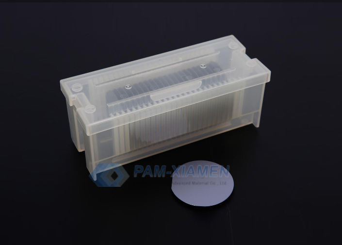
| Packing | single in alufoil |
Remark: for Orientation, we can offer on axis or off axis such as (100) 6deg. toward <111 B>
For more information, send us email at victorchan@powerwaywafer.com and powerwaymaterial@gmail.com