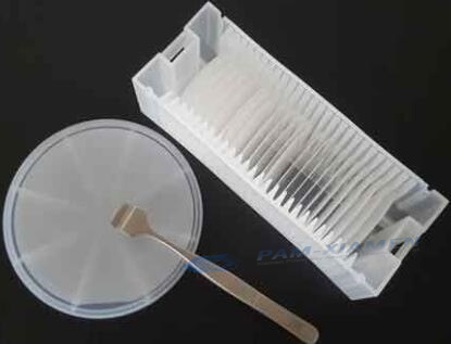
GaN LED structure grown on nano-scale patterned sapphire (Al2O3) substrate can be provided with high efficiency of photoluminescence and electroluminescence. However, because of the high customization of the epitaxial process in the InGaN/GaN-quantum wells based LED heterostructure, we cannot get the optimal solution for patterned sapphire substrates. The design of patterns is ever-changing, and there will be no convergence in the design of patterned sapphire substrates in the future. Typical pattern shapes include cones, domes, square cones or trigonal cones. Even though academic research shows that the smaller the pattern size (100-1000nm), the better the light efficiency, but the LED industry still dominates with 3-4um patterns for growing InGaN/GaN LED structure and working on gallium nitride micro LED devices. Spec of double side polished GaN PSS wafer from PAM-XIAMEN as below:
1. Specification of InGaN / GaN LED Structure on Sapphire Substrate
PAM160506-LED
| 1
|
Supply & Delivery of 2 inch LED GaN epitaxial wafer on PSS (Patterned Sapphire Substrate ) double side polished sapphire substrate
|
| 1-1 | Growth Technique – MOCVD, structure as shown in item3 |
| 1-2 | Wavelength range:450-460nm |
| 1-3 | Substrate Material: |
| 1-4 | flat Sapphire Substrate (Al2O3)-PSS substrate |
| 1-5 | Front side: PSS pattern |
| 1-6 | Backside: Fine ground or Epi-polished roughness ≤ 0.3um |
| 1-7 | Substrate Conduction: Insulating |
| 1-8 | Substrate Orientation: c-Plane (0001) 0.2°±0.1° |
| 1-9 | Diameter: 50.8mm±0.15mm |
| 1-10 | Thickness: 430um±20um |
| 1-11 | High brightness and LED chip specification as listed below |
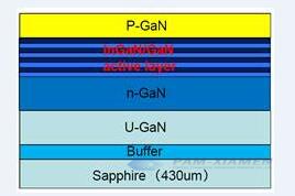
Nitride based LED Structure on Sapphire Schematic Diagram
Features:
High uniformity and good repeatability
2. GaN based LED Chip
LED chip using the above GaN LED wafer should have following specification.
(Based on 10mil*23mil chips, ITO process)
| Parameter | Condition | Symbol | Spec. | Yield |
| Forward Voltage | If=20mA | Vf | ≤3.4V | ≥90% |
| Reve
se Leakage Current |
Vr= -8V | Ir | ≤1μA | ≥90% |
| Reverse Voltage | Ir=10μA | Vr | ≥15V | ≥90% |
| Range of Dominant Wavelength | If=20mA | △λd | ≤7.5nm | ≥70% |
| Radiant Flux | If=20mA | Po | ≥23mW@455nm | ≥70% |
| ESD (HBM) | —— | ESDV | ≥2000V | ≥70% |
The LED chip fabrication process should be:
a) Clean Indium Ball: after you get our wafers, you need to clean indium ball for the next process;
b)ICP etch;
c)Etching, making electrode;
d)Evaporation;
e)Rough grinding;fine grinding (grinding the sapphire substrate to 100um);
f)Laser cutting;
g)Point measurement; Testing (mainly test wavelength/light intensity/VF).
3. Epitaxial Growth of InGaN/GaN Quantum Well Blue LED Structure
A dry etching mask is grown on a sapphire substrate, and the mask is patterned with a standard photolithography process. The sapphire is etched using ICP etching technology, and the mask is removed. And then GaN material is grown on it to make the vertical epitaxy of the GaN material becomes the horizontal epitaxy. As for the etching, it (dry etching/wet etching on the C plane sapphire) is used to design and produce micro-level or nano-level patterns with specific rules of microstructure on the sapphire substrate to control the output light form of the GaN LED devices. Actually, the concave-convex pattern on the sapphire substrate will produce light scattering or refraction effect to increase the light output. At the same time, GaN thin films grown on patterned sapphire substrates will produce a lateral epitaxial effect, reduce the gap defect between GaN and sapphire, improve the quality of epitaxy, and improve the internal quantum efficiency of the LED and increase the light extraction efficiency. Compared with LEDs grown on flat sapphire substrates, PSS can increase the brightness of LED nanostructured device by more than 70%.
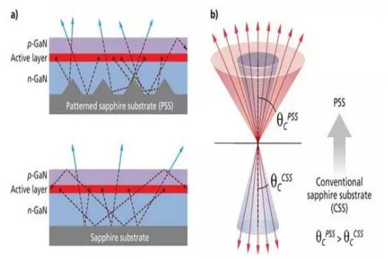
4. How does the Patterned Substrate Improve the LED Light Extraction Efficiency?
The PSS can scatter the photons outside the total reflection cone into the total reflection cone, thereby improving the light extraction efficiency, which is specifically as Figure a). This effect is equivalent to increasing the critical angle of photon overflow shown as Figure b). Studies have found that GaN based light-emitting diodes grown on PSS can increase the light extraction efficiency by up to 30%.
The patterned sapphire substrate improves the epitaxial growth of nitride LEDs by reducing the misfit dislocations, and the reduction of this misfit dislocation is caused by the patterned sapphire substrate to increase the lateral growth, that is, the growth parallel to the substrate surface. Misfit dislocations generally pass through traditional flat sapphire substrates or patterned sapphire
The substrate occurs during the initial epitaxial growth of the nucleation stage. Many researchers have used transmission electron microscopes to find that by improving the lateral composition of the GaN LED structure epitaxial growth on patterned sapphire substrate, misfit dislocations can be reduced.
Because electrons and holes (combination) undergo non-radiative recombination at the dislocation line, the reduction of misfit dislocations in the active layer is one of the most important factors to improve the light conversion efficiency (also known as internal quantum efficiency). Generally, by improving the quality of the epitaxial quantum well, the patterned sapphire substrate can increase the internal quantum efficiency by about 30% for GaN-on-Sapphire LEDs. Of course, the size, shape, quality of the pattern and the optimization of the GaN LED structure epitaxial growth performance matching various pattern designs all have a great influence on the improvement of the internal quantum efficiency of the patterned sapphire substrate.
5. FAQ about Nitride Epitaxy Wafers for LED
Q1: Do you have blue/green nitride wafer structures with superlattices below the MQWs as well?
A: Yes, the standard nitride structures must be grown with superlattices, otherwise the electricity would be weak.
Q2: Do you also provide nitride epitaxy wafers with annealed ITO as a p-contact?
A: we can offer GaN LED wafers with annealed ITO as a p-contact, but it needs >=35wafers.
Q3: For the GaN LED epi stack that you provide, what will be the ideal metallization scheme for the pGaN and nGaN ?
A: The ideal electrode material for the pGaN and nGaN of LED epitaxial wafer should be gold.
Q4: Also are the pGaN:Mg and nGaN:Si layers of LED wafer already activated ?
A: No, you can activate the pGaN:Mg and nGaN:Si layers of LED epiwafer with high temperature equipment at XX ℃ for XX minutes. For the specific values please contact our sales team victorchan@powerwaywafer.com.
Q5: Could you please confirm with the technical personnel the specific lighting method for GaN LED wafer? I’m not sure because I haven’t tried using a wafer to light it up before. If I use a probe station, how can I apply voltage to both p and n layers?
A: After the sapphire substrate is laser lifted-off from GaN LED wafer, the uGaN thickness should be removed by about 2 micrometers to reveal n layer. The principle of lighting up is to make a pn junction, where p is connected to the positive and n is connected to the negative. Just make sure to remove a certain thickness of uGaN and expose n layer after stripping.

For more information, please contact us email at victorchan@powerwaywafer.com and powerwaymaterial@gmail.com.