We are an expert of semiconductor wafers in semiconductor industry, and we offer technology support and wafers selling for thousands of univerisities and industrial customers by our decades experience, including Cornell University, Stanford Univeristy,Peking University, Shandong Univerity, university of south carolina,Caltech Faraon lab (USA),University of California, Irvine (USA),Singapore MIT Alliance for Research and Technology Centre (SMART),West Virginia University,Purdue Univerity, University of California, Los Angeles,King Abdullah University of Science & Technology,Massachusetts Institute of Technology,University of Houston,University of Wisconsin,University of Science and Technology of China etc.
And now we show one article example as follows, who bought our wafers or service:
Article title:
Published by:
Ishaq Ahmad;M. Madhuku;Adeela Sadaf;Shakil Khan;Javaid Hussain;Awais Ali;D. Wan;S.Z. Ilyas;G. Mola;Abdul Waheed;Muhammad Asim Rasheed.
a National Center for Physics, Quaid-i-Azam University, Islamabad 44000, Pakistan
b iThemba LABS, National Research Foundation, P. Bag X11 WITS 2050, South Africa
c Physics Department, Allama Iqbal Open University, Islamabad, Pakistan
d Department of Metallurgy and Materials Engineering, Pakistan Institute of Engineering & Applied Sciences (PIEAS), Islamabad 45650, Pakistan
e Center for Micro and Nano Devices, Department of Physics, COMSATS Institute of Information Technology, Islamabad, Pakistan
f School of Materials Science and Engineering, Shanghai University, Shanghai, China
g School Chemistry & Physics, University of Kwazulu-Natal, Pietermaritzburg Campus, Private Bag X01, Scottsville 3209, South Africa
h Department of Physics, Islamia College Peshawar (Public sector University), Pakistan
Picture of InGaN/GaN Wafer:
Abstract
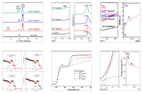
In this study, the influence of Si ions irradiations (12 MeV energetic) on structural and optical characteristics of InGaN/GaN thin film has been investigated. Irradiation was performed at different Si ions fluences in the range of 1×10¹³ to 1×10¹⁵ ions/cm2. X-ray diffraction (XRD) pattern of pristine film indicates only the (0 0 2) oriented crystallites of InGaN while the irradiated films patterns showed other phases (InN and GaN) as well. Ion irradiations at different dose rates have shown no or negligible effect on grain size of InGaN except a shift in the peak position which demonstrates the development of tensile stresses. The existence of other phases in the irradiated films patterns is the indication of InGaN phase separation. Defects produced due to irradiation were also confirmed from peak shifting and appearance of new peak at 669 cm−1 in Raman spectra. A decrease in optical bandgap with the increase of ion irradiation dose rate is being reported in this work.
Subject(s): A. SemiconductorA. Thin filmsB. Ions irradiationsC. X-ray diffractionD. Raman spectroscopy.
Article abstract for Using Wafer from Xiamen Powerway Advanced Material Co. Ltd. (PAM-XIAMEN) or Powerway Wafer Co.,Limited
“… Ion beam irradiation induced change in the optical bandgap was also studied. 2. Experimental
details. InGaN/GaN thin film grown on sapphire substrate has been used in this research work.
It was purchased from Xiamen Powerway Advanced Material Co., Ltd., China …”
Source:
https://www.sciencedirect.com/science/article/pii/S1369800117305863#!
About Xiamen Powerway Advanced Material Co., Ltd
Found in 1990,Xiamen Powerway Advanced Material Co., Ltd (PAM-XIAMEN) is a leading manufacturer of compound semiconductor material in China. PAM-XIAMEN develops advanced crystal growth and epitaxy technologies, manufacturing processes, engineered substrates and semiconductor devices. PAM-XIAMEN’s technologies enable higher performance and lower cost manufacturing of semiconductor wafer.
Now PAM-XIAMEN offer GaN material including GaN substrate, GaN on sapphire, InGaN, InN, and AlN epitaxial wafer with a wide range of deposition rates, various doping levels, wide composition ranges, and low defect densities. As well as GaN based LED wafer and AlGaN/GaN HEMT wafer.
PAM-XIAMEN also offer SiC and GaAs/InP material from wafer substrate to epitaxial growth.
Powerway Wafer Co.,Limited is a sub company of Xiamen Powerway Advanced Material Co., Ltd specialize in dealing with overseas orders.
Are You Looking for an Semiconductor wafer?
PAM-XIAMEN is your go-to place for everything wafers, including SiC/GaN/GaAs/InP wafer with wafer or epitaxial wafer, as we have been doing it for almost 30 years! Enquire us today to learn more about the wafers that we offer and how we can help you with your next project. Our group team is looking forward to providing both quality products and excellent service for you! For more information, please visit our website:www.powerwaywafer.com, send us email at tech@powerwaywafer.com or powerwaymaterial@gmail.com.