PAM-XIAMEN, one of LED wafer manufacturers, offers GaN Wafer for Fabricating LED Devices, which is GaN Epi Structure with InGaN MQWs on sapphire substrate, and can be blue or green emission:
1. Specification of GaN Wafer for LED Devices
No1. PAM200614-GAN-LED
size : 2 inch
WD : 455 ± 10nm
[...]
2020-06-02meta-author
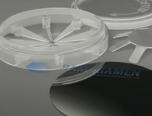
PAM XIAMEN offers 450mm Silicon Wafers.
For more information, please visit our website: https://www.powerwaywafer.com,
send us email at sales@powerwaywafer.com and powerwaymaterial@gmail.com
Found in 1990, Xiamen Powerway Advanced Material Co., Ltd (PAM-XIAMEN) is a leading manufacturer of semiconductor material in China. PAM-XIAMEN develops advanced crystal growth and epitaxy [...]
2019-02-20meta-author
PAM XIAMEN offers 2″ Silicon Wafer.
Material
Orient.
Diam.
Thck
(μm)
Surf.
Resistivity
Ωcm
Comment
n-type Si:P
[100]
2″
200
P/P
FZ 500-1,000
SEMI, , in hard ccassettes of 4, 5 & 5 wafers
n-type Si:P
[100]
2″
500
P/P
FZ >200
SEMI Prime,
n-type Si:P
[100]
2″
225
P/P
FZ >100
SEMI, , Individual cst, 1 very deep scratch
n-type Si:P
[100]
2″
280
P/E
FZ 60-90
SEMI Prime
n-type Si:P
[100]
2″
150
P/P
FZ 50-110
SEMI Prime,
n-type Si:P
[100]
2″
280
P/P
FZ 2-5
SEMI Prime
n-type Si:P
[111-3.5° towards[110]] ±0.5°
2″
279 ±15
P/E
FZ >2,000
SEMI Prime
n-type Si:P
[111] ±0.5°
2″
280
P/P
FZ 2,000-4,000
SEMI Prime, TTV<5μm, Both-sides Epi-Ready
n-type Si:P
[111] ±0.5°
2″
280
P/P
FZ 2,000-4,000
SEMI Prime, TTV<5μm
n-type [...]
2019-03-07meta-author
PAM XIAMEN offers 3″ Silicon Oxide Wafer
3″ Silicon Oxide Wafer
Diameter (mm): 76mm
Grade: Prime
Growth: CZ
Type/Dopant: any
Orientation: 100
Resistivity (Ohm-cm): any
Thickness (µm): 500±25μm
Tolerance (µm): any
Surface Finish: SSP
Flats: SEMI-Std.
TTV < (µm): any
Bow < (µm): any
Warp < (µm): any
Particles [...]
2020-04-24meta-author
PAM XIAMEN offers Cu Coated Silicon.
Cu Film on Silicon Wafer, 4″ , 400 nm Thick, – Cu-Ti on Si-4-400nm
Cu Film on Ta/Silicon Wafer, 4″ , 100 nm Thick, – Cu-Ta-Si-4-100nm
Cu Film on Ta/thermal oxide/Silicon Wafer, 4″ , 400 nm Thick, – [...]
2019-04-26meta-author
PAM-XIAMEN offers (11-22) Plane N-GaN Freestanding GaN Substrate:
Item
PAM-FS-GAN(11-22)- N
Dimension
5 x 10 mm2 or 5 x 20 mm2
Thickness
380+/-50um
Orientation
(11-22) plane off angle toward A-axis 0 ±0.5°
(11-22) plane off angle toward C-axis -1 ±0.2°
Conduction Type
N-type / Si Doped
Resistivity (300K)
< 0.05 Ω·cm
TTV
≤ 10 µm
BOW
BOW ≤ 10 µm
Surface Roughness
Front side: Ra<0.2nm, epi-ready;
Back side: Fine Ground or polished.
Dislocation Density
≤ 5 x 10 6cm-2
Macro Defect Density
0 cm-2
Useable Area
> 90% (edge exclusion)
Package
each in single wafer container, under nitrogen atmosphere, packed in class 100 clean room
For more information, please contact us email at victorchan@powerwaywafer.com and powerwaymaterial@gmail.com
2020-08-20meta-author