Photoluminescence-based material quality diagnostics in the manufacturing of CdZnTe ionizing radiation sensors
A photoluminescence method was used for characterization of crystalline perfection of CdZnTe single crystals in the different stages of an up-to-date process of ionizing radiation sensor production. It was shown that the point method is an effective tool for diagnostics of technology-induced defects and structural irregularities, which can have substantial effect on the sensor performance. From the photoluminescence spectrum, one can obtain information about nature and relative concentrations of initial (as-grown) and technology-induced defects as well as about their interaction. Therefore, the photoluminescence method gives the possibility to correct technological regimes and thus support high quality of the material and high spectrometric (energy resolution, sensitivity) performance of sensor devices.
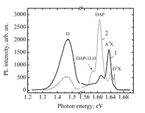
Fig. 1. LTPL spectra of Cd0.9Zn0.1Te crystals registered at 5 K: 1, undoped sample; 2, indium doped sample (with a dopant concentration of 8 × 1016 cm−3) .
Source: Sensors and Actuators A: Physical
If you need more information about Photoluminescence-based material quality diagnostics in the manufacturing of CdZnTe ionizing radiation sensors, please visit our website:https://www.powerwaywafer.com/, send us email at sales@powerwaywafer.com or powerwaymaterial@gmail.com.