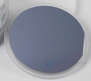
Terahertz (THz) wave generation technology is widely used in fields such as terahertz sensing, safety imaging, non-destructive material testing, and high-speed terahertz wireless data communication. Optical heterodyne is a method of achieving continuous tunable terahertz wave emission by mixing beat frequency signals of two laser modes with different wavelengths of light. It is considered a simple and effective solution. Uni-traveling carrier photodiodes (UTC-PDs), as optical mixer components, are key components in optical heterodyne processes for achieving ultrafast O-E conversion in the terahertz frequency range. A modified uni-traveling carrier photodetector (MUTC-PD) design with a hybrid absorber section has been proven to have faster response speed and higher O-E conversion efficiency compared to traditional UTC-PD designs. PAM-XIAMEN can produce MUTC-PD epiwafers based on InP substrate, specific structure of MUTC photodetector please refer to the table below:

1. MUTC Photodetector Layer Structures
PAMP22175 – MUTC-PD
No.1 MUTC Photodetector Epi-structure
| Layer No. | Material | Thickness | Doping Concentration(cm-3) |
| 20 | p-InP:Zn | – | – |
| 19 | p+-InGaAs:Zn | – | – |
| 18 | p+-InGaAsP:Zn(Q1.15um) | – | – |
| 17 | p+-InGaAsP:Zn(Q1.40um) | – | – |
| 16 | p+-InGaAs:Zn | – | – |
| 15 | p+-InGaAs:Zn | – | – |
| 14 | i-InGaAs | 0.01um | – |
| 13 | n-InGaAsP:Si(Q1.50um) | – | – |
| 12 | n-InGaAsP:Si(Q1.15um) | – | – |
| 11 | n+-InP:Si | – | – |
| 10 | n-InP:Si | – | – |
| 9 | n+-InP:Si | – | – |
| 8 | n+-InGaAsP:Si(Q1.30um) | – | – |
| 7 | n+-InP:Si | – | 1×10¹⁸ |
| 6 | n+-InGaAsP:Si(Q1.30um) | – | – |
| 5 | n+-InP:Si | – | – |
| 4 | i-InP | – | – |
| 3 | n+-InGaAs:Si | – | – |
| 2 | n+-InP:Si | – | – |
| 1 | i-InGaAs | – | – |
| 0 | SI InP Substrate | Fe-doped |
No. 2 MUTC-PD Epitaxial Layers
| Layer No. | Material | Thickness | Doping Concentration(cm-3) |
| 22 | p-InP:Zn | – | – |
| 21 | p+-InGaAs:Zn | – | – |
| 20 | p+-InP:Zn | – | |
| 19 | p+-InGaAsP:Zn(Q1.10um) | – | – |
| 18 | p+-InGaAsP:Zn(Q1.40um) | – | – |
| 17 | p+-InGaAs:Zn | – | – |
| 16 | p-InGaAs:Zn | – | – |
| 15 | n-InGaAs | – | nid |
| 14 | n-InGaAsP:Si(Q1.50um) | – | – |
| 13 | n-InGaAsP:Si(Q1.15um) | – | – |
| 12 | n+-InP:Si | – | – |
| 11 | n-InP:Si | – | – |
| 10 | n-InP:Si | 0.1um | – |
| 9 | n+-InP:Si | – | – |
| 8 | n+-InGaAsP:Si(Q1.30um) | – | – |
| 7 | n+-InP:Si | – | |
| 6 | n+-InGaAsP:Si(Q1.30um) | – | – |
| 5 | n+-InP:Si | – | – |
| 4 | i-InP | – | – |
| 3 | n+-InGaAs:Si | – | – |
| 2 | n+-InP:Si | – | – |
| 1 | i-InGaAs | – | – |
| 0 | SI InP Substrate | Fe-doped |
2. About MUTC-PD
Typically, UTC-PD is composed of a P-type light absorption layer and an N-type wide bandgap junction layer, with only electrons as active carriers. Due to the much higher electron mobility than hole mobility, the drift speed of electrons has a significant advantage. Compared to the accumulation effect of holes in photodiode, higher incident light intensity is required to cause the accumulation effect of electrons in photodiode (i.e. threshold light intensity). Therefore, UTC photodiode can effectively suppress the space charge effect, which also allows UTC photodetector to maintain high-speed signal output under high incident light intensity and high current conditions.
MUTC photodiode structure is an improvement on the UTC structure to enhance high power capability and responsiveness while maintaining high bandwidth. By inserting an appropriately thick undoped InGaAs layer between the unexhausted InGaAs absorption layer and the InP drift layer, the responsivity of the UTC photodiode can be increased. The InP drift layer is doped with n as a charge compensation layer to reduce the space charge shielding effect at high current densities. The charge compensation layer pre distorts the built-in electric field to achieve a flat electric field distribution at high current density.
A typical MUTC photodetector structure operating at 1550 nm wavelength includes several main components, including a heavy p-doped InGaAs absorption layer and a light n-doped InP electron collection layer. The thin undoped InGaAsP layer between the absorption layer and the collector layer forms a graded bandgap transition. In the MUTC-PD structure, a portion of the absorber will undergo mild n-doping and will be completely depleted under appropriate reverse bias. Compared with traditional UTC-PD, photo generated carriers are accelerated by the strong electric field generated in the depletion region, which accelerates the response speed of MUTC PD.
For more information, please contact us email at victorchan@powerwaywafer.com and powerwaymaterial@gmail.com.

